AI Server Backplane PCBs: Laminate, Impedance and Press-Fit Trade-Offs
- Peter
- 926 reads
AI server backplanes hinge on laminate loss, impedance control, via stubs and press-fit hole quality. Here's how those choices interact in practice.

An AI server backplane PCB is where a lot of the system's electrical and mechanical compromises finally become visible. It carries computing modules, GPU expansion hardware, storage devices and power interfaces through one shared board, and every signal that crosses it has to survive connector transitions, long traces and tight alignment tolerances. Get the laminate, via structure or hole tolerance wrong and the failure shows up as a link that won't train at full speed, not as an obvious fault.
EBest Circuit (Best Technology) manufactures multilayer PCBs and provides component sourcing, assembly and testing. In backplane projects, the practical approach is to review board construction and assembly requirements together, from laminate selection and plated holes through connector placement and the finished deliverable.

Where the Backplane Sits in the Server
A backplane is a central interconnection board. Modules plug into it, and it routes traces, connectors and power-distribution structures between them, so each module doesn't need its own point-to-point cable run. Its job changes with the architecture, and it's common to find these boards in AI and GPU servers, NVMe storage systems, modular compute systems, blade chassis, network switching systems and server power distribution.
A single backplane may carry PCIe, Ethernet, storage, management and power at once, and each of those interfaces brings its own electrical rules. A PCIe storage backplane, for example, fans out to multiple SSDs over high-speed differential links, and the layout has to handle connector transitions, trace loss and the specific PCIe generation in use.
One caveat worth keeping in mind: in some AI server designs, GPU-to-GPU traffic doesn't pass through the backplane at all. It runs over dedicated switch boards, module substrates or cable assemblies. The backplane's role has to be defined by the system's interconnect architecture, not assumed from the name.
Backplane Versus Motherboard
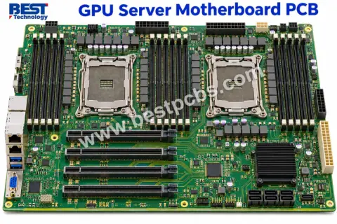
An AI server motherboard hosts the processors, memory interfaces, controllers and other primary components. A backplane mostly connects separate compute, storage or expansion modules. Both can be dense multilayer structures, but their routing priorities pull in different directions.
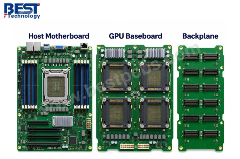
| Feature | AI Server Backplane | AI Server Motherboard |
|---|---|---|
| Main function | Connects hardware modules | Hosts computing components |
| Main features | Connectors and interconnects | CPUs, memory, controllers |
| Routing priority | Module-to-module signals | Chip-to-chip signals |
| PCB construction | Often thick and multilayer | Dense multilayer |
| Key challenge | Signal loss and alignment | BGA routing and power integrity |
| Assembly | Press-fit and SMT | Primarily SMT |
A motherboard typically lives or dies by dense BGA breakout, fine-pitch placement and local power delivery. A backplane tends to have longer transmission paths, large connector arrays and tighter mechanical alignment requirements. That's why a board that looks fine as a motherboard can underperform as a backplane: the loss budget is spent on the trace, not the chip package.
Passive or Active: Which Does Your Server Need?
A passive backplane connects modules electrically without switching or regenerating the signal. An active backplane adds ICs that perform retiming, switching, monitoring or management.
A passive design works when direct connections meet the channel requirements. Its traces and connectors carry signals, power and ground planes distribute current, and there are fewer active parts to cool, maintain or assemble. It may still carry passive resistors and capacitors.
Active backplanes bring in PCIe switches for fan-out, retimers or redrivers for signal conditioning, storage-management controllers and power-monitoring or status circuitry. The trigger is usually a channel that exceeds its allowable loss budget. A retimer can restore signal quality on that link, but it costs board space, power, thermal headroom and component integration effort.
My read: start from the channel budget. If the simulated link closes with a passive design, the simplicity usually wins. Reach for an active design when conditioning, switching or management is a functional requirement, not a fix for a layout that should have been tightened first.
PCB Backplane or Cable Backplane?
A PCB backplane routes signals as copper traces in a rigid multilayer board. A cable backplane sends selected signals through cable assemblies. The PCB version offers compact integration and integrated power planes. Cables can win on long, high-speed links where trace loss becomes the dominant problem.
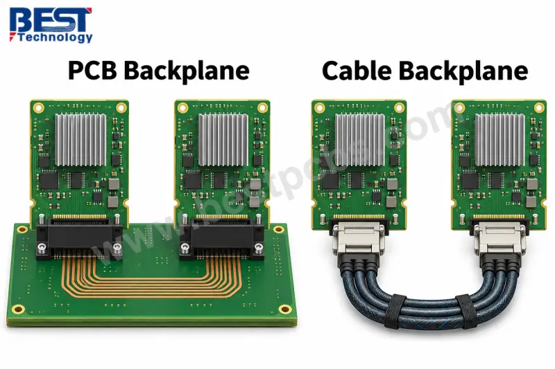
| Factor | PCB Backplane | Cable Backplane |
|---|---|---|
| Signal path | PCB copper traces | Cable conductors |
| Main advantage | Compact integration | Lower loss on some long links |
| Mechanical structure | Rigid board | Flexible routing |
| Power distribution | Integrated planes | Often separate power paths |
| Installation | Board and connectors | Cable assembly and routing |
| Typical use | Dense modular systems | Long high-speed connections |
Some AI servers combine both. A rigid board handles power and management, while high-speed cables carry the selected data links. Either way, the decision should come from complete channel simulations that include connector and transmission-medium losses, not from a rule of thumb about trace length.
Laminate Selection: Where the Loss Budget Starts
AI server backplanes commonly use high-Tg FR-4, low-loss, or ultra-low-loss laminates. The right choice depends on signal frequency, transmission length, loss, thermal requirements and layer count. Two electrical properties do most of the work:
- Dk (dielectric constant) influences propagation and the geometry needed for a target impedance.
- Df (dissipation factor) indicates dielectric loss at a specified frequency. Lower values generally reduce dielectric attenuation.
Two thermal and mechanical properties matter just as much. Tg characterizes the glass-transition behavior of the laminate, and CTE affects dimensional stability and plated-hole reliability through thermal cycling.
Common backplane laminates
| Laminate | Typical Dk at 10 GHz | Typical Df at 10 GHz | Tg |
|---|---|---|---|
| FR408HR | 3.65 | 0.0095 | 190°C |
| I-SPEED | 3.63 | 0.0060 | 180°C |
| I-TERA MT40 | 3.45 | 0.0031 | 215°C |
| TACHYON 100G | 3.02 | 0.0021 | 215°C |
High-speed families from Panasonic (MEGTRON) and Isola (Tachyon) each span multiple grades. Treat the values above as typical figures and check the specific grade's datasheet before locking a stackup, because the numbers shift between grades and test conditions.
Copper foil matters too. Surface roughness adds loss at high frequency because current crowds toward the conductor surface. Low-profile or very-low-profile foil is often specified for the critical high-speed layers.
Hybrid stackups put different dielectrics in one board: low-loss material around the critical signal layers, and other materials where cost or power distribution is the priority. Before approving one, the fabricator should check lamination compatibility, resin flow and bonding, differences in thermal expansion, copper and dielectric spacing, and finished thickness and dimensional stability. For complex backplanes, material choice belongs with the stackup design, not in a purchasing spreadsheet.
Layer Count and Board Thickness
Layer count follows from routing density, connector pin assignments, reference-plane needs and power distribution. Finished thickness depends on the stackup, connector specification, mechanical rigidity and plated-hole manufacturing limits. There's no standard count for AI server backplanes.
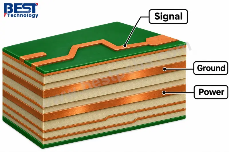
A complex server backplane may need separate layers for high-speed differential pairs, ground references, power distribution, low-speed management signals and connector breakout transitions. As an example, a 24-layer design might place several signal layers between ground planes, with power and management routing taking the remaining layers. More layers add routing capacity, but they also raise fabrication cost, lamination complexity and inspection effort.
Thickness matters most when large press-fit arrays are involved. A thicker board is stiffer, but it lengthens the through-hole barrels and adds via-stub effects. Before approving a thickness, check the connector-approved board thickness, press-fit pin engagement, plated through-hole aspect ratio, drilling and plating capability, finished flatness and mechanical support during insertion. Review the stackup and connector specification together before production drawings are final.
What Governs Signal Integrity Across the Board
Signal integrity in a backplane is the combined behavior of traces, vias, connectors, reference planes and dielectric. Each adds attenuation, reflection or coupling, and the sum must stay inside the interface's channel budget. The five factors that show up most often are controlled impedance, insertion loss, return loss, crosstalk and differential skew.
Controlled impedance. Typical nominal targets are 50 Ω for many single-ended lines, 85 Ω for certain PCIe differential designs and 100 Ω for many other differential interfaces. The actual target comes from the interface specification. Trace width, spacing, copper thickness, dielectric height and Dk all move the number. A 100 Ω differential pair with ±10% tolerance has an acceptance window of 90–110 Ω.
Insertion loss. This is the attenuation through the channel, expressed in decibels at specific frequencies. Long copper runs, dielectric loss, copper roughness, connector transitions and via discontinuities all contribute. On long backplane channels, a lower-loss laminate and tuned trace geometry are the main levers.
Return loss. Reflections come from impedance discontinuities: abrupt trace transitions, connector launches, via geometry and unused via stubs. Cutting discontinuities keeps impedance consistent and protects signal quality.
Crosstalk. Energy from one path couples into a neighbor. Differential-pair spacing, reference planes, routing arrangement and connector pin assignment are the usual controls.
Differential skew. When the two conductors of a pair have different propagation delays, skew results. Length mismatch, dielectric variation and routing geometry all contribute. Follow the skew limit for each interface rather than applying one universal length-matching rule.
Evaluate the complete path through channel simulation and, where needed, S-parameter measurements.
Backdrilling: Removing the Stub Without Cutting the Contact
When a signal uses only part of a plated via, the leftover barrel becomes a via stub. That unused copper reflects signal energy and degrades high-speed transmission. Backdrilling removes the excess from the unused end while keeping the copper that makes the needed connection. The stub here is a piece of unused copper, not an electrical short.
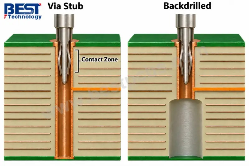
Depth control is the hard part. Drill too shallow and residual stub remains. Drill too deep and you cut into copper that the connection needs. Fabrication drawings should state the drilling side, target depth and maximum allowable residual stub length.
Press-fit holes need extra care. Press-fit pins depend on the plated barrel for both electrical contact and mechanical retention. If backdrilling removes copper from the pin's contact zone, the electrical connection and long-term reliability of the connector can suffer. The drill program has to protect that zone explicitly.
What Backplane Connectors Need From the PCB
Backplane connectors depend on accurate finished-hole dimensions, reliable copper plating and precise alignment. High-density press-fit connectors are the most demanding case for drilling, plating, board thickness and flatness.
A press-fit pin is compliant. It deforms as it enters a plated through-hole, and the resulting contact pressure gives both electrical connection and retention without a solder joint.
| Parameter | Requirement |
|---|---|
| Finished hole diameter | Connector-specific tolerance |
| Hole copper plating | Approved thickness and quality |
| Hole position | Accurate pin-array alignment |
| PCB thickness | Within connector specification |
| Board flatness | Suitable for connector seating |
| Backdrilling | Preserve the contact region |
Hole diameter is one of the tightest controls. An undersized hole raises insertion force and can damage the barrel. An oversized hole reduces contact pressure and retention. Follow the connector manufacturer's application tolerance.
Plating defines the contact surface. Microsection inspection can confirm copper thickness, plating continuity and internal-layer connections.
Alignment and support matter because large arrays generate significant insertion force. The board needs support locations, mounting features and clearance for insertion tooling. Check connector position and flatness during dimensional inspection. For high-speed connectors, follow the recommended footprint, ground-via arrangement and signal-launch geometry to hold channel performance.
How the Backplane Carries Power
A power-carrying backplane moves current through connector contacts, copper planes or traces, and vias. Resistance anywhere along that path causes voltage drop and heating, so the narrowest copper section isn't the only possible bottleneck. The two relationships to keep in view are:
ΔV = I × R
P = I² × R
Here ΔV is voltage drop in volts, I is current in amperes, R is the resistance of the path in ohms, and P is dissipated power in watts.
As an illustration, a 20 A path with 2 mΩ of resistance drops 0.04 V and dissipates 0.8 W. At 40 A through the same resistance, the drop becomes 0.08 V and dissipation rises to 3.2 W. Doubling the current quadruples the heating, which is why power paths get disproportionate attention in thermal review.
Wider copper, additional layers and suitable via arrays reduce board resistance. Connector contact ratings and temperature rise belong to the same analysis. Current sharing between parallel contacts depends on connector construction and routing, so multiplying one contact's rating by the contact count can overstate real capacity. Some servers route main power through separate distribution boards or busbars, and a signal backplane carrying only local auxiliary power shouldn't be sized for full system current.
How AI Server Backplanes Are Tested
Testing combines electrical inspection, impedance measurement, structural analysis and dimensional verification. High-speed designs may also need channel measurements for insertion and return loss.
| Test Method | Main Verification |
|---|---|
| Electrical test | Opens and shorts |
| TDR | Controlled impedance |
| Microsection | Plating and layer structure |
| AOI | Copper pattern defects |
| X-ray | Selected internal features |
| Dimensional inspection | Holes, thickness, alignment |
| VNA | High-frequency channel behavior |
Electrical testing confirms intended connections exist and unintended ones don't. It matters most on large boards with dense connector arrays and many nets.
TDR measures transmission-line impedance. Using the same example as before, a 100 Ω differential specification at ±10% accepts 90–110 Ω. Measurements usually run on representative impedance coupons under the approved test method.
Microsection gives a cross-sectional view. It checks plated-hole copper thickness, inner-layer interconnection, layer alignment, dielectric spacing, and backdrilling depth and residual stubs.
AOI and X-ray serve different purposes. AOI finds copper-pattern defects such as opens, shorts and spacing deviations during fabrication. X-ray examines internal structures that optical methods can't see.
VNA measurements are used for critical high-speed channels. S-parameters characterize insertion loss, return loss and other transmission properties, and the results are compared against the approved channel specification.
EBest Circuit's Backplane Capabilities
EBest Circuit combines multilayer PCB fabrication, engineering review and coordinated assembly for server hardware. The company says its engineering review catches manufacturing concerns before fabrication, which can cut avoidable revisions and schedule slips.
Per EBest Circuit, its FR-4 PCB capabilities cover standard builds from 1 to 10 layers and special-process builds up to 32 layers. For 1 oz copper, the listed standard inner- and outer-layer trace/space is 4/4 mil (approximately 0.10/0.10 mm), with 3/3 mil available through special processing. Designs with 8 or more layers use high-Tg material under the company's fabrication requirements.
For backplane projects, the review covers stackup feasibility and material availability, via structures and plated-hole aspect ratios, backdrilling depth and residual stub limits, press-fit hole specifications, impedance requirements and test coupons, and tolerances and inspection access.
On the assembly side, the company lists Yamaha YSM20R placement equipment, 3D SPI, nitrogen reflow, wave soldering, AOI and X-ray inspection. For active backplanes, that lets fabrication and component assembly be reviewed together. Prototype, low-volume and repeat orders are all supported, and actual capability and lead time are confirmed after reviewing layer count, material, thickness, drilling structure and test requirements.
Gerber or ODB++ files, stackup, connector specifications, target impedance, quantities and test requirements can be sent to [email protected] for an engineering review and quotation.
FAQ
What's the difference between a midplane and a backplane?
A midplane usually connects modules mounted on opposite sides of a central board, while a backplane generally provides connections behind a group of modules on one side. Product naming varies, so the mechanical arrangement and connection diagram define the actual layout.
Can one backplane support SATA, SAS and NVMe drives?
Some backplanes do, but the connectors, lane routing and controller must support each protocol used. A board designed only for SATA or SAS doesn't gain NVMe support just because the drive fits the bay.
Are U.2, U.3 and EDSFF backplanes interchangeable?
Generally not. U.2 and U.3 compatibility depends on the drive, backplane and controller implementation, and EDSFF uses different defined form factors and connector arrangements. The platform's supported-drive list is the practical reference for any replacement.
Does every AI server backplane support hot swapping?
No. Hot swap needs suitable connectors, power-control behavior and support from controller, firmware and operating system. A removable drive or module isn't automatically safe to insert or remove while powered.
Does an AI server backplane always need HDI?
No. Conventional through-hole multilayer construction can suit many backplanes. HDI becomes useful when dense connector fields or fine-pitch active components need interconnections that through vias can't accommodate efficiently.
Can a faster backplane upgrade an older server?
Not by itself. The host, endpoints, connectors, cables and firmware all have to support the intended interface generation. A newer backplane can't push the link rate past what the connected devices support.
The Takeaway
An AI server backplane has to hold reliable high-speed transmission, controlled multilayer construction, accurate connector interfaces and stable power distribution at once. Laminate loss, impedance, via stubs, board thickness and press-fit hole quality all feed into the finished board's behavior, and they're tightly coupled. Settle the channel budget and connector specification first, then lock the stackup and material around them. Changing the laminate late usually means changing the impedance, the thickness and the drill program with it.