GPU Server Motherboard PCB: How Connection Method Sets Layers, Materials and Cost
- Peter
- 726 reads
How a GPU server connects its accelerators sets the motherboard's lane budget, layer count and laminate choice. Here's how those decisions chain together.
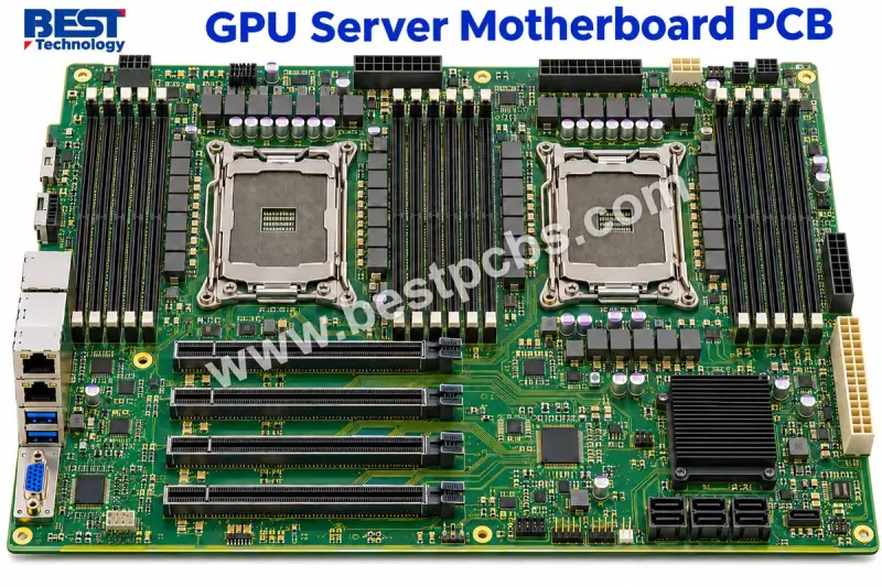
In a GPU server, the way accelerators connect to the host decides most of the motherboard's design before anyone picks a laminate or a layer count. Some systems plug GPU cards straight into PCIe slots or risers on the host board. Others hand the accelerators to a separate GPU baseboard. Those two approaches produce very different PCBs, and mixing them up is one of the easier ways to scope a custom server project wrong.
The GPU connection method sets the lane budget, the routing density, the stackup and the power path. Direct PCIe connections need enough CPU lanes and routing space on the host board. A separate baseboard moves part of the GPU interconnection off the motherboard, which shifts the PCB problem somewhere else. Working through the connection method first keeps the rest of the board decisions honest.
EBest Circuit (Best Technology) provides multilayer PCB fabrication, component sourcing and assembly for custom electronic hardware. Our engineering team reviews board construction and assembly files so a motherboard design can move into prototype and production builds without re-scoping at each step.
What a GPU Server Motherboard PCB Actually Carries
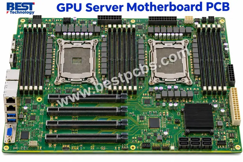
A GPU server motherboard PCB is the multilayer board that hosts the processor, memory and system interfaces for a GPU-equipped server. Copper traces carry signals between devices, power and ground planes distribute current and return paths, and dielectric layers keep the copper separated. The bare board becomes a motherboard only after sockets, connectors, voltage regulators and other parts are installed.
The key point is what the board doesn't carry. A motherboard in this class usually doesn't host the GPU chips. Its layout includes direct GPU slots, riser connectors or cable connectors that lead to a separate accelerator assembly. That's why a request for an "8 GPU server motherboard" needs a clarifying question: does the customer want a host board that serves an accelerator assembly, or a PCB with eight GPUs physically mounted on it? The system block diagram answers that, and it tells you which board needs fabricating.
Typical applications include AI training servers that move data between host processors, storage and several accelerators; inference servers that combine GPU processing with network and storage interfaces; high-performance computing systems running simulation and parallel workloads; and rendering servers that host multiple GPU cards in a rack-mounted chassis. The broader AI server PCB family also includes accelerator boards, network boards and power distribution boards, each with its own manufacturing role.
Host Motherboard, GPU Baseboard or PCIe Card
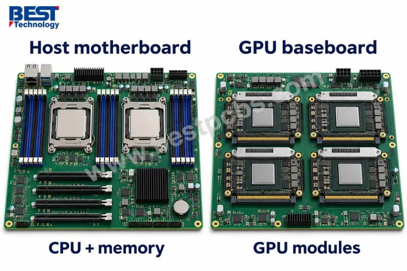
Three board types show up in these designs, and they're easy to blur together. The host motherboard handles the CPU, system memory and server I/O. A GPU baseboard connects accelerator modules to each other and to the host, following the requirements of that particular GPU platform. A PCIe GPU card puts the GPU, its local memory, its voltage regulators and its PCIe interface on one card that plugs into a slot or riser.
| Board type | Main components | Main connection role |
|---|---|---|
| Host motherboard | CPU sockets, DIMM sockets, management circuitry and system connectors | Connects host processing, memory, storage, networking and GPU interfaces |
| GPU baseboard | GPU module connectors, power circuitry and, on some platforms, dedicated interconnect switches | Connects accelerator modules to each other and to the host system |
| PCIe GPU card | GPU, local memory, voltage regulators and PCIe interface | Adds an accelerator through a PCIe slot or riser |
Each choice changes the host board's job. With a baseboard architecture, the motherboard may route less GPU traffic but still needs the host-side interfaces and power inputs. With direct slots, the motherboard takes on the full PCIe routing burden, which is where the lane count and layer count start to climb.
Lane Budgets: Counting Before Routing
Server motherboards connect multiple GPUs through CPU PCIe links, either directly, through risers, through PCIe switches, or through baseboard connections defined by the accelerator platform. How many GPUs you can use depends on available lanes, the connection topology and what the system firmware supports.
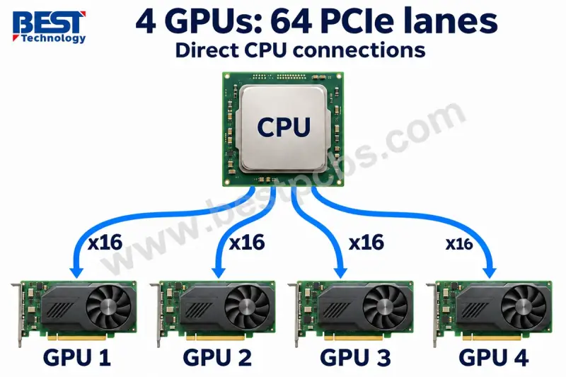
Direct connections give each GPU its own link, and the CPU's lane count sets the widths available. Risers let you relocate cards to fit the chassis, and a single riser may carry one link or several. PCIe switches fan out multiple downstream devices from fewer upstream CPU lanes, but the upstream link then carries shared traffic, and bandwidth drops when the combined demand exceeds that connection's capacity. Baseboards supply the module connections and interconnect layout that the chosen accelerator platform requires.
For full-width direct connections, the arithmetic is simple:
GPU PCIe lanes = number of GPUs × lanes per GPU
Four GPUs each running at x16 need 4 × 16 = 64 lanes, and that's before NVMe drives, network adapters and other devices take their share. This is the first number to check, because it may rule out a CPU or a topology before anyone opens a layout tool. A switch-based design can reduce upstream lane demand, but it trades that for shared bandwidth, so the workload has to tolerate it.
Don't trust the connector to tell you the width. A physical x16 slot can be wired for x8 operation, and a compatible device will then run on the narrower link. The electrical configuration on the board is what counts, not the length of the slot.
Layer Count Follows Routing, Not GPU Count
The layer count comes from the routing demands of the CPU, memory and PCIe links, plus whatever reference planes and copper the power distribution needs. The number of GPUs is a poor predictor on its own. Four GPUs with a simple switch topology may need fewer layers than two GPUs with dense direct routing from the CPU.

Several pressures drive the stackup. CPU sockets and memory channels consume routing space around dense pin fields. PCIe links need room for differential pairs and separation from neighbouring signals. Ground planes give high-speed signals nearby return paths. Power layers distribute several rails without forcing current through narrow copper. And board thickness has to stay compatible with the connectors, sockets and plated-hole manufacturing the design requires.
Say a proposed 20-layer board runs short of routing space. Adding signal layers can relieve the congestion, but each new signal layer needs a proper reference plane and dielectric spacing, or the added layers just create new impedance problems. Moving to 22 layers only makes sense when the revised stackup solves a specific routing or power requirement you can name.
The stackup document should show each layer's function, copper thickness and finished dielectric thickness. Those numbers feed impedance calculations and the fabrication drawing, so they need to be right before quoting. Our AI server PCB design guide covers how those stackup choices connect to signal integrity and power delivery.
Laminate Choice: Loss, Dk and Tg Are Different Questions
High-Tg FR-4 can suit less demanding channels. Low-loss laminates become the better candidates when routes run long, interfaces get faster or several connectors eat into the signal-loss budget. The right answer depends on the complete channel, not on the word "server" in the spec sheet.
Four properties do most of the work:
- Df, the dissipation factor, describes dielectric loss and feeds into signal attenuation.
- Dk, the dielectric constant, affects impedance and propagation delay.
- Tg, the glass transition temperature, marks the point where the resin's mechanical behaviour changes as temperature rises.
- Copper roughness affects conductor loss, and its effect grows at higher frequencies.
High Tg and low loss are separate properties, and this is where teams get caught. A thermally robust FR-4 grade can still carry too much electrical loss for a demanding PCIe channel. Choosing by the Tg number alone is the mistake to avoid.
The MEGTRON 6 examples below show how much the exact construction matters, even inside one material family:
| Material grade | Glass type | Typical Dk at 13 GHz | Typical Df at 13 GHz | Tg by DSC |
|---|---|---|---|---|
| R-5775(N) | Low-Dk glass | 3.34 | 0.0037 | 185°C |
| R-5775(K) / R-5775(G) | Normal glass | 3.62 | 0.0046 | 185°C |
These typical values come from a 0.75 mm test sample, with Dk and Df measured by the balanced-type circular disk resonator method. Both grades share the same Tg, yet their electrical behaviour differs, which is the whole argument in one table. Impedance calculations still need the dielectric thickness and copper construction of the actual board, so a datasheet value alone won't close the design.
For material selection, our high-speed PCB materials guide walks through the differences between FR-4 and low-loss options. Hybrid stackups, which combine compatible material systems in one board, can make sense for cost and performance. But the materials have to laminate together and expand at compatible rates, or reliability suffers.
PCIe Generation and the Full Channel Budget
Each PCIe generation tightens the margin. Trace length, copper roughness, connectors and via transitions all become more demanding parts of the design as the transfer rate climbs.
| PCIe generation | Transfer rate per lane | Signaling |
|---|---|---|
| PCIe 4.0 | 16 GT/s | NRZ |
| PCIe 5.0 | 32 GT/s | NRZ |
| PCIe 6.0 | 64 GT/s | PAM4 |
GT/s measures the interface transfer rate, not the usable throughput. Encoding and protocol overhead take their cut before any application sees the data. PCIe 6.0 moves to PAM4, which uses 4 signal levels where NRZ uses 2. That change alters the signal-quality requirements at the receiver, so a channel that worked at a lower generation may need rework before it meets the next one.
Signals lose strength across the whole path: motherboard traces, connectors, risers and the GPU card itself. Designing only the board trace misses most of the problem. Sometimes shortening a route or removing an unnecessary layer transition helps as much as changing the laminate.
The practical routing priorities are continuous reference planes, differential-pair geometry matched to the platform's impedance target, and controlled spacing from adjacent signals. Retimers can restore signal timing on channels that need it, but they bring extra components, power and placement requirements of their own. Add them on purpose, not as a fix you hope for after a failed link.
Power Delivery at Low Voltage and High Current
The motherboard takes power through its input connectors and spreads it through copper planes, vias and voltage regulator circuits to the CPU, memory and expansion interfaces. GPU cards or baseboards often have their own power connections for the much larger accelerator loads, so the motherboard's power budget should only count what it actually supplies.
Voltage regulator modules, or VRMs, step the input supply down to the low voltages that processors and other devices need. Low voltage doesn't mean low current. As an illustration, a 200 W load at 1.0 V requires 200 A at the load, from I = P / V.
At those currents, copper resistance stops being a footnote. Take the same illustrative case: 100 A through a 0.5 mΩ path produces a 0.05 V drop and 5 W of heat, from V = I × R and P = I² × R. Here, R is the total resistance of the path under evaluation, including the relevant copper and connections. A 0.05 V drop at a 1.0 V rail is a five percent loss before the load sees anything, which is why power paths get such careful attention.
The layout needs enough copper cross-section, properly sized via connections and short paths between regulators and loads. Narrow necks around pads, cutouts or mounting holes can become bottlenecks even when the surrounding plane looks generous. Check those neck points explicitly rather than trusting the big plane area.
HDI, Via-in-Pad and Backdrilling: Three Different Problems
HDI and via-in-pad help route dense component connections. Backdrilling reduces the electrical effect of unused plated-hole sections. Each process fixes a different problem, and they get conflated more often than they should.
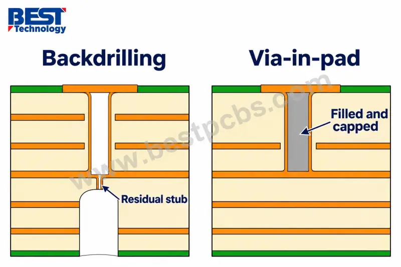
- HDI uses small vias and additional interconnect structures to route dense pin fields where conventional through-holes eat too much space.
- Via-in-pad places the connection inside a component pad, which allows a shorter route to another layer. Solderable pads commonly need filled and capped structures so solder doesn't drain into the hole.
- Backdrilling removes the unused part of a plated through-hole after plating, which cuts the residual via stub on a high-speed signal path.
Picture a through-hole via that connects an outer layer to a nearby inner layer. Through a thick board, it leaves a long unused barrel running to the bottom. That stub can resonate and disturb a high-speed signal. Backdrilling removes most of the unused section and keeps the intended connection intact.
Fine-pitch component routing can justify HDI even on a short signal path. A thick board, on the other hand, may need backdrilling on selected PCIe vias without requiring microvias across the whole design. The pad layout and the channel requirements together show where each process earns its place, so decide them per channel rather than as a blanket rule.
Cooling Hardware and Board Size Shape the Layout
Heat sinks, cold plates and chassis dimensions decide where sockets, memory, connectors and mounting points can go. Those mechanical requirements need space reserved in the layout before routing starts. Moving them afterward can push connectors or cut through copper areas the electrical design already depends on.
The main considerations are these:
- CPU heat sinks need mounting space and clearance from DIMM sockets, power components and cables.
- Air-cooled designs need airflow through the component area, so tall connectors shouldn't block the intended path.
- Liquid-cooled designs need clearance for cold plates, fittings and hoses, plus access during assembly.
- GPU risers and cables must line up with their chassis positions without stressing motherboard connectors.
- Large boards need proper support around heavy heat sinks and at connector insertion points.
Board outline, component height limits and mounting-hole positions belong in the mechanical drawing supplied to the PCB and assembly teams. Lock them early. A late change to a mounting hole can cascade into a re-route, and nobody wants to rediscover that during bring-up.
Assembly and Test Stages That Catch Different Faults
GPU server motherboard assembly needs controlled solder-paste deposition, accurate component placement and a reflow profile suited to large sockets, connectors and areas with very different copper mass. Inspection and electrical testing then check the board stage by stage.
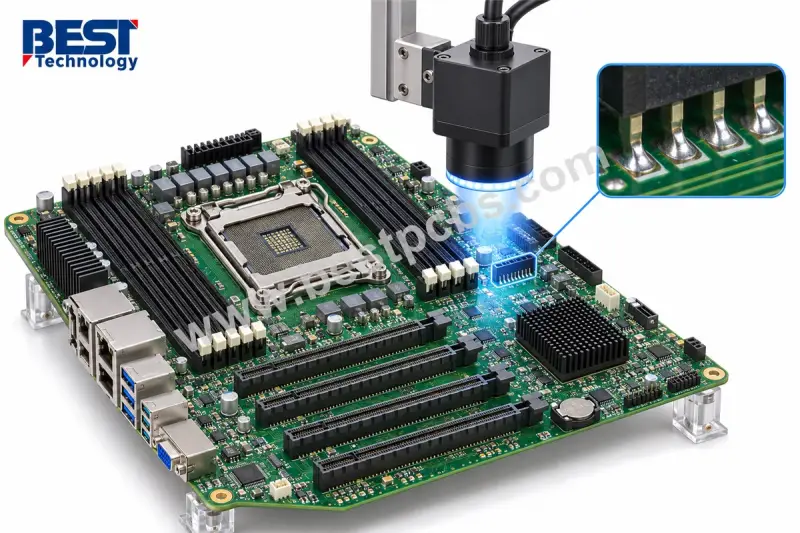
Large connectors and power components absorb heat differently from small surface-mount parts. The reflow process has to form their joints without overheating the more sensitive devices nearby. On big assemblies, board supports help keep the panel flat through printing, placement and soldering, which matters for paste deposits and placement accuracy.
| Production stage | Main checks |
|---|---|
| Bare PCB | Continuity and isolation, dimensions, plated-hole quality and specified impedance coupons |
| Solder-paste printing | Paste volume, alignment and deposits that could cause bridges or insufficient joints |
| After component assembly | Component position, polarity, visible joints and hidden solder connections where X-ray inspection applies |
| Powered functional testing | Voltage rails, startup, memory detection and agreed communication or interface functions |
TDR measures impedance behaviour on the structure it's applied to, which makes it a useful check on the fabricated stackup. But a PCIe link needs more than a coupon measurement. Qualifying the link means running the platform's own electrical and system tests. Passing TDR alone doesn't establish that a link works in the chassis.
For functional testing, the build plan should name the CPUs, memory, firmware, fixtures and procedure. That lets the assembly supplier quote and perform a defined test, rather than promising "fully tested" with no agreed scope behind it.
Manufacturing Capabilities for Motherboard Builds
EBest Circuit brings bare-board fabrication, component sourcing and assembly into one project. That helps keep the board construction and the parts and processes for the finished motherboard in step, instead of managing them as separate handoffs.
Our FR-4 PCB manufacturing capabilities include the following process options:
| Manufacturing item | Capability |
|---|---|
| Layer count | 1–10 layers in the standard process; special-process builds up to 32 layers |
| Material requirement | High Tg material for 8 layers and above |
| Laser via diameter | 0.10 mm |
| Inner-layer trace/space with 1 oz copper | 4/4 mil standard; 3/3 mil with special processing |
| Through-hole aspect ratio | 8:1 standard; 10:1 with special processing |
Our engineers assess the layer count, hole structure and copper geometry together before confirming a special-process motherboard build. Those three interact, so reviewing them separately tends to miss something.
Our PCB assembly services pair manufacturing equipment with support for the customer's component and test requirements:
- Yamaha YSM20R placement equipment handles surface-mount assembly, and 3D SPI checks solder-paste deposits before placement.
- Nitrogen reflow and through-hole assembly processes cover boards that mix small devices with sockets and larger connectors.
- AOI and X-ray inspection examine component placement and solder connections, including joints hidden under suitable package types.
- Customers can use our component sourcing service or supply selected parts, with BOM and incoming-material checks before assembly begins.
- Functional testing can follow an agreed procedure using the firmware, hardware and fixtures the project requires.
For prototype and production orders, we review the fabrication files, BOM and assembly requirements together. That way, material availability, component packages and manufacturing details get resolved before the build starts, not during it.
Frequently Asked Questions
Can an x16 PCIe slot operate with only 8 lanes?
Yes. A physical x16 slot can be wired for x8 operation, and a compatible device can use that narrower connection. At the same PCIe generation, x8 provides half the lane bandwidth of x16, though the practical effect depends on how much data the workload moves over PCIe.
Does a PCIe retimer add more PCIe lanes?
No. A retimer restores signal timing and quality along an existing link. It doesn't create extra CPU lanes, and it isn't a multi-device PCIe switch. Its job is to help a channel meet signal requirements across the planned connection.
Does a custom motherboard PCB order include BIOS or BMC firmware?
Not automatically. Bare-board fabrication supplies the PCB, and assembly installs the specified components. BIOS and baseboard management controller firmware, programming and startup testing need a defined project scope, including the required software files and any licensing arrangements.
Can EBest Circuit assemble a motherboard using customer-supplied components?
Yes. Customers can supply selected components while we source the rest of the BOM. The assembly plan records which parts come from which source, along with package, quantity and handling requirements, before production begins.
Can prototype and production builds use the same stackup?
Yes, provided the materials and construction remain available and suitable for production. Using the intended production stackup for prototypes reduces changes between electrical validation and volume manufacture. A change in material or dielectric thickness can require renewed impedance and channel checks.
Where a Custom Board Project Should Start
GPU server motherboard PCB design starts with the host architecture and the GPU connection method. From there, the lane budget, stackup, laminate, power path and manufacturing process fall into place. Keeping the motherboard, accelerator boards and power paths clearly separated helps you choose the right construction without piling on complexity you don't need.
For a custom motherboard PCB or assembly project, send your fabrication files, stackup requirements, BOM and target quantity to [email protected]. EBest Circuit can review the manufacturing scope with your team and discuss prototype or production options. The first question worth settling is still the lane count, because every other decision downstream depends on it.