Aerospace PCB Impedance Control: Tolerances, Stackups and TDR Verification
- Love PCB
- 834 reads
Impedance targets come from the interface, not the aerospace label. Stackup, materials, rigid-flex transitions and TDR coupons all shape the final result.

Aerospace PCB impedance control comes down to one idea: keep selected signal traces at a defined characteristic impedance by managing their geometry, the dielectric around them and their reference planes. Get that right and RF and high-speed signals pass between components without reflections at every change in the transmission path. Get it wrong and the problem often shows up late, at the receiver, where it's hardest to diagnose.
In avionics, radar, satellite communications and onboard computing, the correct impedance depends on the interface and the board construction. Some nets need tightly controlled transmission lines. Short, slow control signals may not need any of that. Sorting nets into those groups early is the cheapest decision in the whole process.

Start With the Interface, Not the Application Label
The impedance target should come from the interface specification and the channel design. Fifty ohms single-ended and 100 Ω differential are common values, but they aren't universal aerospace requirements. Two interfaces on the same board can need different targets, and treating the whole board as one impedance class is a good way to over-constrain some nets and under-constrain others.
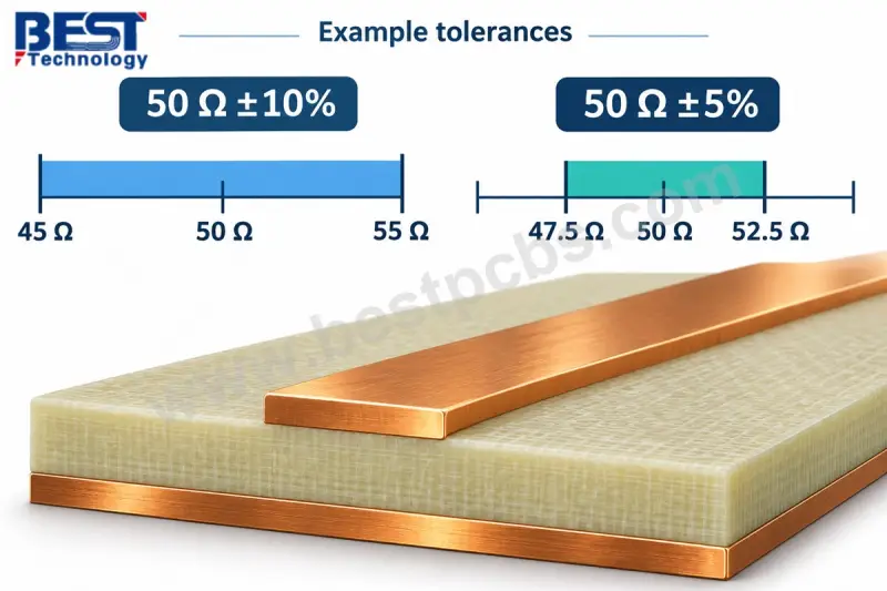
Tolerance matters as much as the nominal value. A 50 Ω trace held to ±10% has a permitted range of 45–55 Ω. Tighten that to ±5% and the window shrinks to 47.5–52.5 Ω. The table below shows how the same nominal values translate into fabrication limits.
| Example requirement | Lower limit | Upper limit |
|---|---|---|
| 50 Ω single-ended, ±10% | 45 Ω | 55 Ω |
| 50 Ω single-ended, ±5% | 47.5 Ω | 52.5 Ω |
| 100 Ω differential, ±10% | 90 Ω | 110 Ω |
| 100 Ω differential, ±5% | 95 Ω | 105 Ω |
Tighter tolerance means tighter control of materials and process, and that usually costs more. My read is that ±5% should be a deliberate choice backed by signal analysis, not a default that gets written into every aerospace drawing. Use ±10% where the interface allows it and save the tighter window for the nets that need it.
The fabrication drawing should tie each target to a signal type and routing layer. A note such as "L3 differential pairs: 100 Ω ±10%, referenced to L2 and L4" gives the fabricator far more to work with than "impedance controlled." Named nets or clear net classes keep those controlled traces distinct from ordinary routing, so nobody has to guess which lines matter.
Deciding Which Nets Actually Need Control
RF paths and digital interfaces with a defined impedance requirement are the obvious candidates. Clock frequency alone is a weak guide, though. A digital signal with a modest clock can still have a fast rising edge, and that edge carries frequency content well above the clock. On a long trace, the reflection from a fast edge can return after the signal has already changed state, distorting what the receiver sees.
A few indicators are worth checking for each net:
- The component or interface documentation specifies a single-ended or differential impedance.
- RF parts connect through a defined system impedance, commonly 50 Ω.
- Fast edges run along long traces, through connectors or across board-to-board interconnects.
- Simulation shows reflections or timing errors that eat into the receiver's operating margin.
Short, slow control lines often work without a controlled-impedance requirement. Flagging the critical nets early keeps the stackup focused on the signals that need it, rather than spreading tight constraints across the whole board.
How Stackup Sets the Impedance
The stackup determines the distance between each signal layer and its reference plane, along with the dielectric properties filling that space. Keep the routed width the same and a different layer construction can still move the result. That's why an impedance model needs the layer-by-layer dimensions rather than a single total board thickness.
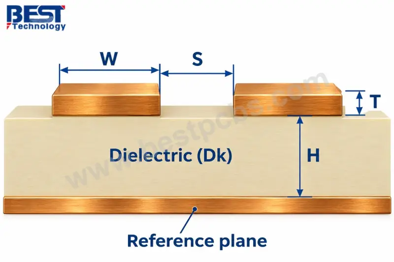
With the other variables held fixed, these trends generally hold:
| Parameter | Meaning | Typical effect when increased |
|---|---|---|
| W | Finished trace width | Lowers characteristic impedance |
| H | Trace-to-reference-plane spacing | Generally raises impedance |
| T | Finished copper thickness | Generally lowers impedance |
| S | Edge-to-edge spacing within a differential pair | Generally raises differential impedance as coupling decreases |
| Dk | Dielectric constant | Generally lowers impedance |
An 8-layer board can put a given signal close to its reference plane or well away from it, depending on how the dielectric thickness is distributed through the stack. Two boards with identical total thickness can have very different impedance behavior.
The difference between PCB core and prepreg matters here. Core is a cured laminate. Prepreg flows and cures during lamination, so its final thickness differs from its unpressed thickness. Impedance calculations need the expected finished dielectric spacing, not the thickness printed on the material sheet before pressing.
Material Choice: Dk Sets Geometry, Df Sets Loss
High-Tg FR-4, low-loss epoxy, RF laminates and polyimide can all serve aerospace projects. Which one fits depends on signal frequency, trace length, operating temperature and whether the board must flex.
- High-Tg FR-4 suits multilayer digital boards that need extra temperature margin, as long as signal loss stays acceptable over the actual trace length.
- Low-loss epoxy systems fit faster or longer digital links where standard FR-4 attenuates the signal too much before it reaches the receiver.
- RF laminates, including hydrocarbon-ceramic and PTFE-based materials, serve microwave paths, antenna feeds and other frequency-sensitive circuits.
- Polyimide covers flexible films for flex circuits and rigid grades for demanding thermal applications.
Dk drives the geometry needed to hit a target impedance. Df, the dissipation factor, governs dielectric loss, which is a separate concern. Two materials can support the same nominal impedance once the trace is resized, yet produce different insertion loss over the same channel. A board can meet its impedance target and still lose too much signal, so long or fast links may need a lower-loss material even when the geometry checks out.
When comparing high-speed PCB materials, look at Dk and Df at the relevant test conditions and frequencies, copper roughness, the dielectric thicknesses actually available and thermal properties. Datasheet comparisons only mean something when the test methods and frequencies line up.
Hybrid builds offer a middle path. An RF laminate on selected layers with FR-4 elsewhere keeps the specialized material where it earns its cost. The catch is that the full material combination has to survive the intended lamination process.
Microstrip or Stripline
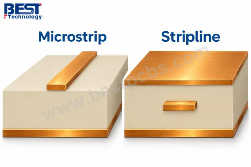
Microstrip suits RF traces running on the outer surface, while stripline suits internal routing where reference planes above and below shield the signal from nearby circuitry. Neither structure has a single standard width for 50 Ω. Each needs dimensions calculated for its own dielectric and copper construction.
| Feature | Microstrip | Stripline |
|---|---|---|
| Signal location | Outer layer above a reference plane | Internal layer between 2 reference planes |
| Surrounding dielectric | Board dielectric plus air or a surface coating | Laminate surrounding the conductor |
| Solder mask influence | Relevant when the trace is coated | Normally not part of the internal trace structure |
| Component access | Direct surface connection is possible | Surface components generally require via transitions |
| Shielding | More exposed to surrounding circuitry and objects | Reference planes above and below help shield the signal |
The trade-off is straightforward. Microstrip keeps components directly accessible but exposes the trace to its surroundings, including solder mask and nearby objects. Stripline shields the signal well but forces vias for every surface connection, and those vias bring their own impedance transitions.
Calculating Trace Impedance
Trace impedance comes from the trace width, copper thickness, dielectric thickness, Dk and the reference-plane arrangement. A trace impedance calculator gives a sensible starting estimate for dimensions. For differential pairs and other structures a basic calculator simplifies, a field solver or detailed simulation is the better tool.
For a uniform, low-loss transmission line, the basic relationship is:
Z₀ ≈ √(L′ / C′)
Where Z₀ is characteristic impedance in Ω, L′ is inductance per unit length in H/m and C′ is capacitance per unit length in F/m.
Take L′ = 250 nH/m and C′ = 100 pF/m:
Z₀ ≈ √[(250 × 10⁻⁹) / (100 × 10⁻¹²)] = 50 Ω
The formula shows the underlying relationship, but it won't hand you a routing width from a laminate datasheet. A real aerospace model needs the actual layer geometry, Dk, finished copper thickness and any solder mask or coverlay. Those inputs should be locked down in the fabrication stackup before final routing dimensions are released. If the fabricator changes a dielectric thickness or material grade, the line width and pair spacing may have to move with it.
Vias, Return Paths and Discontinuities
Vias and interrupted return paths create local impedance changes. A route can have every straight section on target and still reflect energy at its transitions. The complete path includes those transitions, not just the line width between them.
High-frequency return current follows the reference plane directly beneath the signal. A split or void under the route forces that current to detour, enlarging the loop and changing the connection's electrical behavior. Common layout problems include:
- Routing across a reference-plane split or a large clearance opening.
- Changing signal layers without a suitable return path between the relevant planes.
- Leaving a long unused via barrel beyond the layers that carry the signal.
- Introducing large pads, abrupt neck-downs or connector launches that differ sharply from the adjoining line.
When a signal changes layers between planes at different potentials, nearby ground vias that tie those planes together give the return current a shorter route.
Backdrilling removes the unused via barrel and can reduce stub effects in demanding high-speed channels. Shorter vias, blind vias or different layer assignments may reach the same performance without it, so the decision belongs to the channel analysis rather than habit.
Impedance Across Rigid-Flex Transitions
Rigid and flex sections need separate impedance models. The same trace width can give different impedance on each side because the dielectric materials and layer spacing differ. The rigid section usually has glass-reinforced laminate and internal reference planes. The flex section uses polyimide film, adhesive and coverlay, which change the dielectric environment above and below the conductor.
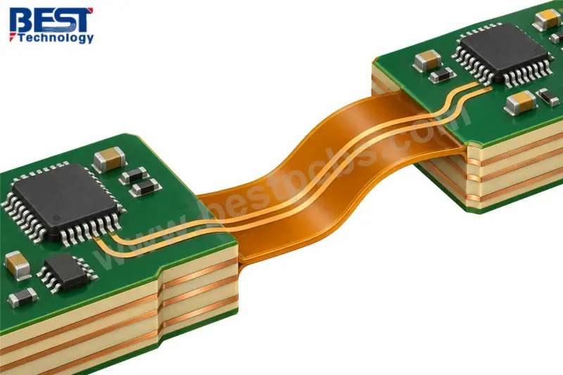
The calculation should account for:
- The polyimide, adhesive and coverlay thicknesses in the flex section.
- The distance from each signal trace to its reference plane in both sections.
- Whether the flex reference plane is solid copper or hatched.
- The width and spacing required on each side of the rigid-to-flex transition.
A 100 Ω differential pair, for example, may need different dimensions in the rigid and flex regions to hold the same target. Keep both traces together through the transition, and don't let either one cross a gap in its reference plane. Those two rules prevent most of the trouble I see in these builds.
Verifying With TDR Coupons
Time-domain reflectometry, or TDR, checks impedance by launching a fast electrical step into a test structure and measuring the reflected response. The instrument converts that response into an impedance profile that can be compared against the specified limits.
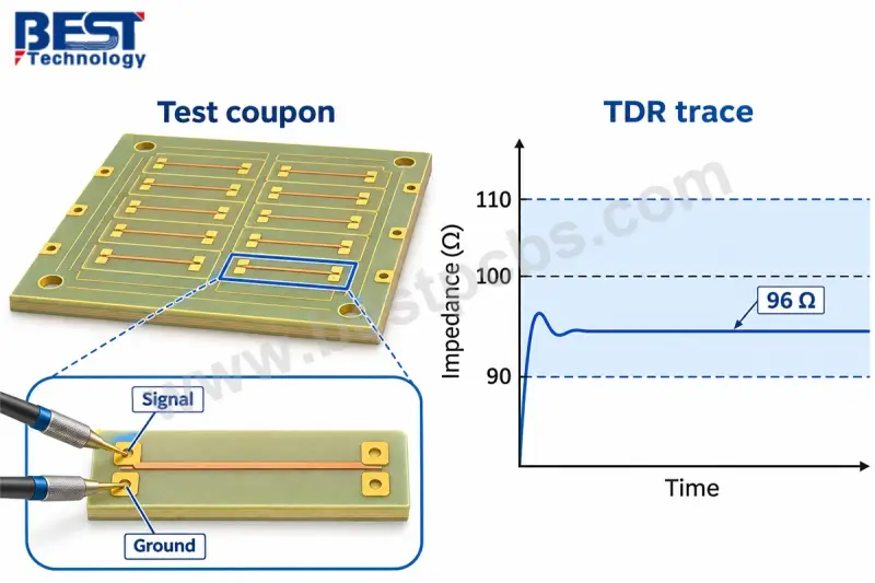
Fabricators usually test coupons built on the same panel as the boards. A coupon reproduces the signal layer, trace geometry, dielectric construction and reference structure, and it gives the probe accessible contact points. A useful impedance report identifies:
- The board or panel lot and its associated coupon.
- The tested layer and whether the structure is single-ended or differential.
- The nominal impedance and permitted tolerance.
- The measured result and pass/fail status.
- The measurement window and test conditions needed to interpret the trace.
Take a 100 Ω differential requirement with ±10% tolerance. A measured 96 Ω falls inside the 90–110 Ω range. A reading of 112 Ω falls outside it, and that calls for investigation of the construction, the processing or the measurement setup before anyone accepts the lot.
A coupon verifies the manufactured transmission-line structure. It doesn't cover connector launches, routing discontinuities or total channel loss, which need their own design or system-level checks. The broader inspection and documentation requirements around the finished board are covered in our guide to aerospace PCB testing requirements.
Common Questions From Design Teams
Can a continuity test verify controlled impedance?
No. Continuity confirms that a connection exists. Impedance testing measures transmission-line behavior, so a trace can pass continuity and still miss its target.
Does solder mask change microstrip impedance?
Yes. Mask changes the dielectric environment around a surface trace and generally lowers its impedance compared with the uncoated geometry. Coated microstrip models should include the mask properties and thickness.
Does 100 Ω differential impedance mean each trace is 50 Ω?
Not necessarily. Trace spacing changes how the two conductors interact. Two traces designed separately for 50 Ω may not form a 100 Ω pair when placed close together, so the pair has to be calculated as a pair.
Can a PCB pass its impedance coupon and still have signal-integrity problems?
Yes. The coupon tests a representative structure, not the entire assembled channel. Excess channel loss, crosstalk, poor termination or discontinuities elsewhere in the route can still cause failures.
Does changing copper weight require a new impedance calculation?
Yes. Copper thickness affects impedance, so the trace width and pair spacing should be recalculated for the new copper specification.
Can the same trace width be kept after a laminate substitution?
Only if the revised model still hits the target. A replacement material can change Dk, available thicknesses or lamination behavior, so width and spacing need rechecking against the new build.
Where EBest Circuit Fits In
EBest Circuit (Best Technology) describes its controlled-impedance support as covering PCB fabrication, material selection, stackup review and impedance testing, with assembly available when a customer needs a complete PCBA. The company says its manufacturing experience spans more than 20 years across PCB and electronic assembly work.
- The company manufactures multilayer FR-4 boards and high-frequency constructions for digital, RF and mixed-signal designs.
- Its Rogers PCB capabilities cover RO4003C, RO4350B, RT/duroid 5880 and Rogers/FR-4 hybrid constructions.
- Before fabrication, the company reviews controlled layers, reference planes, dielectric spacing and conductor dimensions against the requested electrical targets.
- Impedance testing runs alongside the agreed inspection requirements, so the manufactured structure can be verified before assembly or integration.
- Prototype, production and assembly work can be coordinated through the same manufacturer.
What to Lock Down Before Release
Aerospace impedance control starts with the interface target and then works backward through materials, layer spacing and trace geometry. Each net needs its own tolerance, each stackup change needs a recalculation, and each rigid-flex transition needs its own model. TDR coupons confirm the result, but they only confirm the structure they represent.
Before release, make sure the Gerber files, intended stackup, impedance targets, tolerances and applicable quality requirements all agree with each other. A mismatch between the drawing and the stackup is the most common way a controlled-impedance board goes wrong, and it's far cheaper to catch on paper than on the bench.