Seat Belt Buckle Switch PCB Design, Assembly and Testing Requirements
- zeng, liuyan
- 494 reads
Buckle sensor PCB production depends on matching board geometry, sensing method and test limits to the mechanical assembly.

A buckle switch PCB has to do two jobs at once: provide the specified electrical signal and fit inside a mechanism whose moving parts must still latch and release correctly. That makes board thickness, locating features, sensor position and test access part of the functional design. A circuit that passes a continuity check can still fail in the buckle if its contact geometry or sensor alignment is wrong.
Seat belt buckle switches detect whether the belt tongue is latched. Depending on the vehicle design, that signal can support belt reminders, restraint-system decisions or electronic parking-brake logic. The switch does not independently control airbag deployment, and not every buckle switch contains a PCB.

Three PCB roles inside a buckle switch
A buckle switch board may provide a conductive pattern for a moving contact, carry a Hall sensor and its associated circuitry, or connect switch terminals, resistors and external wires. Each construction puts different demands on fabrication and inspection.
- Contact-pattern boards: The moving contact touches conductive areas on the PCB. Contact geometry, plating and surface cleanliness matter alongside the board’s solderable features.
- Hall-sensor boards: A mounted sensor detects a magnetic field as the buckle changes state. Sensor orientation and position relative to the magnet are key assembly dimensions.
- Interconnection boards: The board connects terminals, resistors and wiring. Circuit integrity, component values and terminal attachment need to match the approved design.
The mechanical buckle retains the belt; the PCB supports state detection. A wire or switch in the assembly doesn’t by itself reveal how the internal electronics are built.
Board thickness can decide whether the design fits. EBest Circuit lists regular thickness ranges of 0.4–3.5 mm for ENIG boards and 0.6–3.5 mm for HASL boards, subject to layer count and the full construction. A 0.4 mm board is within the stated ENIG range but outside the regular HASL range. In a tight housing, that difference can affect the stack-up and the space available around the latch.
A usable mechanical definition should identify locating edges, mounting holes, component-height limits and wire exits. These features establish whether the populated board fits without interfering with the buckle mechanism.
Mechanical contacts and Hall sensing need different tests
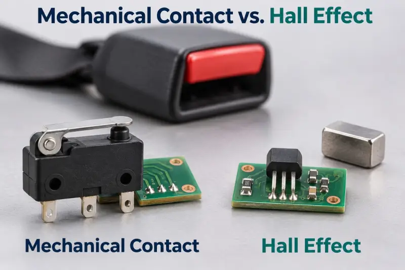
Mechanical-contact and Hall-effect switches produce different electrical behavior, so their test methods and limits can’t be swapped. The figures below describe specific Littelfuse designs; they are examples, not ratings for every buckle sensor.
| Item | Mechanical-contact example | Hall-effect example |
|---|---|---|
| Switch behavior | Normally open; closes when latched | Two current-output logic states |
| Electrical specification | Maximum switching voltage: 12 VDC | Powered magnetic sensing; supply depends on the selected configuration |
| Current specification | Closed-state sensing current: 5–30 mA | Typical low output: 5.0 / 6.9 mA; typical high output: 12.0 / 17.0 mA |
| Operating temperature | −40°C to +85°C | −40°C to +85°C |
| Assembly relationship | Contact travel and engagement | Sensor orientation and magnetic geometry |
The Hall output figures are listed as typical values, and the selected configuration must be established before setting test limits. They’re not directly comparable to the mechanical design’s specified sensing-current range: the figures describe different electrical quantities.
For a mechanical design, review contact geometry and finish, along with any resistor-coded circuit. If the moving contact touches the PCB itself, the solder-pad finish specification doesn’t define the contact surface’s wear performance.
For a Hall design, define sensor orientation, magnet position and the relationship to the housing datum. A continuity check can’t verify current output. Likewise, a sensor’s −40°C to +85°C rating doesn’t automatically qualify the complete assembled board over that range.
Fabrication choices and contact finishes
EBest Circuit lists FR4 options in standard, medium and high-Tg grades, with a regular range of 1–10 layers. The material and stack-up should follow the specified thermal and assembly requirements. Tg describes a material transition; it isn’t the assembly’s allowable continuous operating temperature.
| Manufacturing item | Listed process range | Design check |
|---|---|---|
| ENIG board thickness | 0.4–3.5 mm | Housing fit and assembly support |
| OSP board thickness | 0.4–3.5 mm | Soldering sequence and storage |
| HASL board thickness | 0.6–3.5 mm | Pad geometry and thickness compatibility |
| Finished hole diameter | 0.20 mm regular; 0.15 mm special process | Review vias and terminal holes together |
| Through-hole aspect ratio | Up to 8:1 regular; 10:1 special process | Check board thickness against hole diameter |
Within this process specification, boards above eight layers require high-Tg material. Special-process values need engineering confirmation against the complete design; they shouldn’t be combined into a board specification without a manufacturability review.
ENIG, OSP, immersion tin and other surface finishes can be assessed against the pad layout and assembly process. ENIG offers a flat solderable surface. OSP calls for attention to handling, storage and soldering sequence.
If a moving contact uses the PCB as its electrical surface, define the plating system, thickness, contact area and acceptance criteria directly. A solderable finish doesn’t establish contact wear performance, and a hard-gold finger capability doesn’t automatically qualify a different contact shape. When protective coating is required, drawings should specify coverage and keep-out areas for contacts, connectors and test points.
DFM and assembly checks
Design-for-manufacturing review needs to cover the bare board and its position in the finished buckle. Set a mechanical datum for critical holes, slots, sensor locations and board edges so that fit can be measured against the housing.
- Clearance: Include component height, solder joints, wire exits and moving parts. Check both sides of the board.
- Sensing geometry: Mark contact zones or the Hall sensor’s required orientation. Supply relevant housing and magnet information when it affects placement acceptance.
- Panel handling: Allow room for assembly support and fiducials. Keep separation features and their mechanical stress away from sensitive components and functional edges.
- Test access: Reserve connections for power, ground and required output measurements before housing, coating or wires make them difficult to reach.
The review should resolve open engineering questions against a controlled drawing revision. Specify tolerances for the locating relationships that matter rather than applying tighter tolerances indiscriminately across the board.
For assembly, the BOM, component-location drawing and placement-coordinate file need to agree. Sensor part numbers, resistor values, connector pin numbering and polarity all affect the finished circuit. A proposed component substitution needs customer approval if it can change electrical output or magnetic response.
Stencil design and reflow conditions depend on the board and components. Small boards may need a panel or carrier for printing, placement and reflow. EBest Circuit lists solder paste inspection (SPI) for printed deposits, AOI for visible placement and solder features, and X-ray inspection for hidden joints when the component package and inspection plan warrant it.
Wire attachment, connector soldering, cleaning, coating and depanelization should be included in the agreed build scope when needed. Document wire length, stripping dimensions, exit direction and strain relief. Electrical checks and positional checks catch different problems: a correctly soldered sensor still has to occupy the position and orientation required by the mechanism.
Dimensional and functional quality control

EBest Circuit lists these regular-process dimensional references for FR4 boards:
| Inspection item | Regular-process reference | Inspection focus |
|---|---|---|
| Board outline dimension | ±5 mil (±0.127 mm) | Finished profile against the approved drawing |
| Non-plated hole diameter | ±2 mil (±0.0508 mm) | Specified locating or mounting hole diameter |
| Plated hole diameter | ±3 mil (±0.0762 mm) | Finished diameter after plating |
For a 20.00 mm outline with an approved ±0.127 mm tolerance, the inspection limits are 19.873–20.127 mm. That’s a calculated example, not a buckle product specification. Hole-diameter tolerance doesn’t define hole position; the drawing needs separate requirements for locating relationships.
Electrical and assembly checks address different defects:
- Bare-board electrical test: Check continuity and isolation against approved circuit data before components limit access.
- SPI and AOI: Inspect paste deposits, visible component placement, polarity and solder features. These checks don’t establish sensor function.
- X-ray: Inspect hidden solder joints when the selected package can’t be adequately checked optically.
- Functional test: Apply the specified supply and mechanical or magnetic stimulus, then record the output in both latched and unlatched conditions.
A current-output Hall sensor needs a minimum and maximum output window for each condition. Typical datasheet values aren’t production pass/fail limits. For resistor-coded contacts, use the specified resistance windows rather than assuming a closed switch must read zero ohms. The test plan should identify fixture responsibility, coverage and required records.
Mechanical cycling, environmental qualification and vehicle-system validation are separate from routine PCB and solder-joint inspection. The PCBA process also needs controlled solder-paste printing, component placement and reflow, with inspection data used to investigate deviations. See PCBA process control for further detail.
Prototype timing and quote preparation
EBest Circuit lists standard FR4 prototype references of 7 days for one layer, 8 days for two layers and 10 days for four layers. Its fastest listed services are 24 hours for one- and two-layer boards and 48 hours for four-layer boards, subject to confirmation. These are bare-board references, not delivery commitments for a populated assembly.
The timing references apply to prototype orders below 1 m² using standard FR4, 0.4–1.6 mm thickness, H/H or 1 oz copper, lead-free HASL, green solder mask and white silkscreen. They also specify trace width and spacing greater than 8 mil, holes greater than 0.3 mm and annular rings greater than 10 mil. ENIG, specialized contact plating, smaller features or other constructions need a separate schedule review.
For an assembled board, schedule readiness depends on the bare boards, full component kit, approved assembly data and any functional-test fixture. Assembly, inspection and shipment preparation follow once the necessary inputs are ready; transit time is separate.
A useful quotation package identifies whether the request covers bare boards, populated boards, or added wire and connector work. Include fabrication files and a drawing, stack-up, material, copper thickness, finish and dimensional tolerances. For assembly, provide a BOM with manufacturer part numbers, placement data, assembly drawings and approved alternatives.
Also include the housing envelope, mounting references, component-height limits, contact or sensor position, electrical interface, output limits, test procedure, fixture availability, quantity, packaging and requested delivery date. If the design is still changing, mark unresolved details so confirmed requirements can be assessed separately.
For a manufacturing review, EBest Circuit asks customers to provide the board revision, BOM, quantity, test scope and target delivery date. Confidential design files can be discussed alongside PCB NDA considerations before the full package is shared.
Compatibility questions to settle early
Does every buckle switch contain a PCB? No. Internal construction varies; a PCB is used where the design needs a conductive contact pattern, mounted sensing electronics or an interconnection platform.
Does a different spelling of “seat belt” indicate a different sensor? No. Compare sensing technology, dimensions, electrical interface and application specification to assess compatibility.
Can the same PCB accept another Hall sensor? Only after checking footprint, pinout, supply requirements, output behavior and magnetic characteristics. Package fit alone doesn’t establish electrical or sensing equivalence.
Can a resistor value change without updating the assembly requirements? A resistor may set output coding or support diagnostics. A value change needs design approval and a BOM update; affected test limits also need review.
The practical takeaway is to define the board, buckle geometry and acceptance test as one connected design package. That gives fabrication and assembly teams measurable requirements for fit, sensing behavior and inspection before the first build.