Aerospace BGA Assembly: Design, Reflow and Inspection Controls
- Love PCB
- 638 reads
Aerospace BGA builds depend on package-specific design review, controlled reflow, hidden-joint inspection and traceable acceptance criteria.

For aerospace hardware, a BGA’s stated pitch says little by itself about whether its joints will be manufacturable and acceptable. The work depends on the package and board design, moisture handling, solder paste, reflow conditions, inspection coverage and records required for the specific build. EBest Circuit lists BGA assembly capability down to 0.25 mm pitch, subject to review of the package, board construction and inspection requirements.
That distinction matters: a placement limit is not a reliability rating, and a successful power-up does not establish the condition of every joint hidden under the package. Design data, process evidence and acceptance criteria need to fit together before production starts.

Set the build scope before production
EBest Circuit describes a project scope that can combine bare-board fabrication, component sourcing, surface-mount assembly, X-ray inspection and specified functional testing. Its assembly options include consignment, partial turnkey and full turnkey builds. The manufacturing site, customer requirements and qualification evidence still need review for each order.
The company lists a Yamaha YSM20R placement machine, SINIC-TEK S8080 3D solder paste inspection (SPI), SINIC-TEK A510DL 3D automated optical inspection (AOI), and a UNICOMP AX8200 X-ray system. These are general assembly resources; the applicable inspection coverage and acceptance criteria must be agreed for the product. The stated 0.25 mm BGA pitch and 01005 small-component capability are not, by themselves, aerospace qualification limits.
Package-specific design review is central to that decision. EBest Circuit’s PCB assembly services and PCB design and DFM review describe available services. The proposed build should be assessed against the actual BOM, board data, package drawings and required records.
Check the footprint and board construction
The BGA ball map, ball diameter, land pattern, solder-mask clearances, via construction and board flatness all affect joint formation. Routing space and copper distribution beneath the package also shape the design. A 0.8 mm-pitch part and a 0.4 mm-pitch part can call for different escape routing and stencil choices; pitch alone cannot establish whether a footprint is suitable.
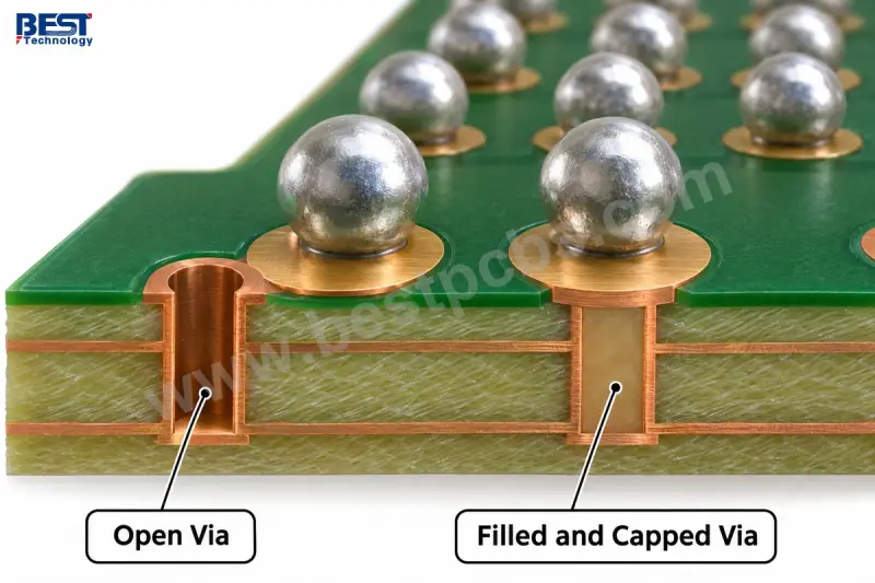
An open via in a soldering land can wick solder away from the joint. If the design uses via-in-pad, the fill, copper cap and finished surface should match the approved fabrication data. A solder-mask tent does not automatically provide the same construction. Board support deserves attention too: flex during handling or depaneling can strain the laminate near BGA pads, and ordinary joint inspection may not reveal resulting damage.
Manage moisture and the soldering process
Moisture-sensitive parts need handling based on their package label, moisture sensitivity level, exposure history and supplier instructions. At receipt, confirm part identity, packaging condition, lot identification and moisture information. Once a moisture barrier bag is opened, track floor life, including for customer-supplied material, and use the specified storage or drying procedure when required.
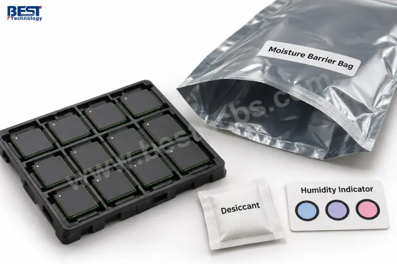
There is no single baking temperature and duration that suits every BGA. Package thickness, exposure and the compatibility of the part’s tray or carrier affect the appropriate treatment. Repeated or unsuitable heating can cause further problems, so follow the applicable component instructions.
Process control links data review to inspection and test. First verify the BOM, orientation, footprint, ball alloy and acceptance requirements. Then select paste and stencil apertures for the package, and measure printed deposits for volume, height, area and offset with SPI. Confirm placement setup and alignment before reflow. Finally, measure the profile on the populated board and apply the agreed inspection and test plan.
Large packages, thick boards, copper planes and nearby components can make uniform heating difficult. The oven’s displayed zone settings do not show the temperature experienced by the hidden joints. Thermocouple positions should capture thermally challenging areas, and the measured ramp, time above liquidus, peak and cooling need to meet the paste and component requirements.

Ball and paste alloys must be considered together. For example, using tin-lead paste with a lead-free BGA requires evaluation of the approved mixed-alloy process and resulting joints; melting the paste alone does not demonstrate acceptance. A hotter profile or nitrogen atmosphere cannot resolve every solderability issue. Reflow self-alignment can help a correctly printed component settle onto its pads, but it cannot reliably correct a wrong footprint, oxidation, substantial placement error or excessive warpage.
Match inspection to the defect
X-ray can show solder bridges, missing balls, solder distribution and detectable voiding. What it reveals depends on defect geometry, image resolution, viewing angle and inspection method. A top-down two-dimensional image may superimpose the ball and paste deposit even when their interface is poorly bonded. Head-in-pillow defects therefore need more than a check that each ball looks round; angled imaging or specialist analysis may be needed, and should be explicitly included in the inspection plan if required.
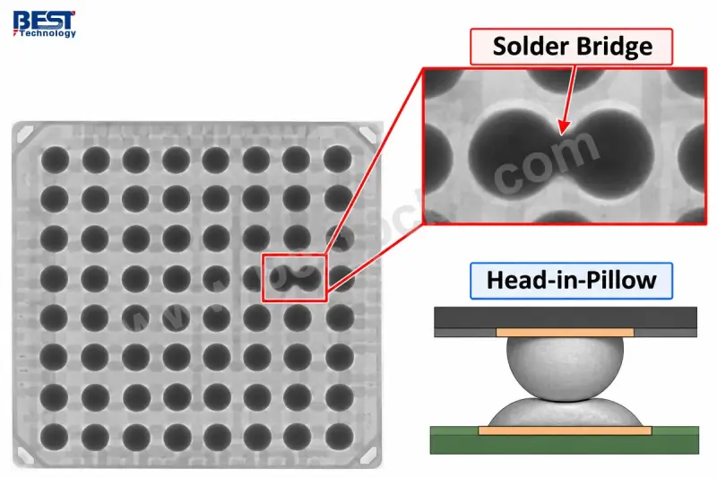
Different defect types point to different investigations. Bridging can relate to excess paste, registration or package movement. Head-in-pillow involves incomplete merging of ball and paste, with warpage, oxidation, flux activity and thermal profile among the factors to examine. Voiding concerns gas retained in the joint; paste behavior, pad and via construction, and profile may be relevant. Pad cratering is laminate fracture beneath or near a copper pad, so board strain, handling, depaneling and material response deserve attention.
One generic void-percentage limit cannot cover every package and product. Define acceptance using the applicable workmanship and product requirements. AOI can assess visible components, orientation and surrounding workmanship, but it cannot directly examine all joints beneath a BGA. Nor does normal continuity or a clean radiograph rule out every laminate crack or latent mechanical weakness.
Agree requirements, records and rework limits
The customer’s requirements and qualification plan determine which standards, revisions, acceptance class, addenda and records apply. J-STD-001 covers soldering requirements, while IPC-A-610 addresses assembly acceptability; applicable addenda may add requirements when specified. AS9100D concerns a supplier’s quality management system and does not itself approve every assembled board for flight use.
EBest Circuit lists AS9100D and ISO 9001:2015 in its quality information. For a proposed order, supplier review should confirm the current certificate, legal entity, manufacturing site and scope. The agreed record set may include component lot identification, moisture exposure records, approved process data, inspection images, test results and a certificate of conformity.
Environmental qualification is a separate activity. Thermal cycling, vibration and other conditions should reflect the hardware’s intended use. A standard functional test does not replace qualification, and the service description does not say that every such test is included in a PCBA build.
Underfill should be selected for the package, board, stress environment, qualification evidence and repair strategy. It changes mechanical behavior and access for rework, so it needs product-specific evaluation. Rework likewise requires agreed permission, process limits, replacement-part controls and post-rework inspection. Replacing a device adds thermal exposure and can affect pads and laminate.
Fine pitch may save routing area, but it can make fabrication, placement, inspection and repair more demanding. The practical choice is the package and board construction that meet the electrical, mechanical and manufacturing requirements together. Provide the approved BOM, PCB and placement data, exact BGA part numbers, quantities and acceptance requirements to [email protected] for a scope review; identify supplier-approval and controlled-data requirements before transferring restricted files.