SiC Gate Driver Board Manufacturing: PCB Limits, Assembly and Testing
- zeng, liuyan
- 700 reads
Custom SiC gate driver boards depend on coordinated PCB construction, component control and inspection, with system-level validation defined separately.
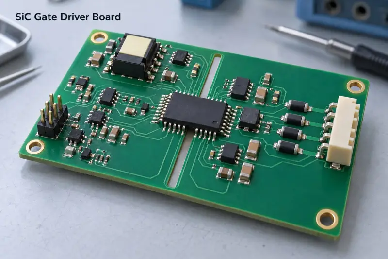
A custom silicon carbide (SiC) gate driver board has to carry the approved circuit into a repeatable physical build. Its PCB geometry, materials, components and assembly process all matter, particularly where the design includes isolated circuits or interfaces with a power module. EBest Circuit offers fabrication, component sourcing, assembly and project-specific testing for customer-designed boards.
The manufacturing package typically begins with Gerber files, a bill of materials (BOM), quantities and the board’s construction requirements. Those inputs allow the fabricator and assembler to review the same revision and identify process constraints before production. Manufacturing review can help catch conflicts in dimensions, footprints or assembly access, but it does not establish the electrical performance of the complete power converter.
Match the board format to the power stage
SiC gate driver boards take several forms. A single-channel board drives one specified switching device, while a half-bridge design provides separate high-side and low-side drive paths. A board built for a SiC power module needs connections that match the selected module interface. Some designs combine gate-drive circuitry with other board functions to reduce the number of separate assemblies.
These configurations describe common project types, not a record of completed customer builds. The actual component set follows the approved design and BOM. It may include isolated power supplies, gate resistors, connectors and protection components where specified.
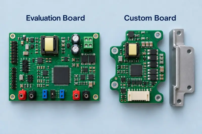
Evaluation boards provide a predefined circuit and mechanical layout for device assessment and application development. A custom board can instead fit a product’s enclosure, connector locations, power-module interface and manufacturing plan. That flexibility comes with engineering, prototype and validation work. A custom design does not automatically cost less or perform better, and an evaluation board may remain suitable after the required assessment.
PCB construction has interacting limits
EBest Circuit lists standard PCB fabrication for 1–10 layers and special processing for 10–32 layers. Available FR4 grades include low-Tg material at 130–140°C, mid-Tg at 150°C, and high-Tg at 170–180°C. Listed copper thicknesses are 0.5–5 oz for standard inner layers and 1–5 oz for standard outer layers.
At 1 oz copper, the listed minimum outer-layer trace width and spacing are 4/4 mil for standard processing and 3/3 mil for special processing. Minimum finished hole diameter is 0.20 mm standard or 0.15 mm under special processing. Standard plated-through-hole diameter tolerance is ±3 mil, with ±2 mil available through special processing. Standard board outline tolerance is ±5 mil; non-plated slot length and width tolerance is ±4 mil.
Listed board thickness ranges vary with surface finish: 0.4–3.5 mm for OSP, ENIG, immersion silver, immersion tin and ENEPIG; and 0.6–3.5 mm for HASL. The available finishes are OSP, ENIG, ENEPIG, immersion silver, immersion tin and HASL.
These figures are process capabilities, not a set of limits that can all be combined freely. Layer count, copper weight, hole size and finished thickness constrain one another. The documented process requires high-Tg material for boards with eight or more layers, and the selected stackup also affects achievable thickness. A DFM review should confirm the complete combination against the required construction.
Fine manufacturing spacing does not define safe electrical separation. Isolation distances may need to be substantially larger than the PCB process minimums, depending on the approved insulation design and its voltage conditions, environment and material properties.
Stackup and isolation geometry need design control
Standard FR4 may suit a design that meets its thermal and insulation requirements. High-Tg FR4 is available for higher-Tg requirements and multilayer construction. Special processing lists higher-CTI laminate options from CTI 400–600 for designs that specify a tracking-resistance material class.
Layer allocation affects routing choices and return paths. A two-layer board has less routing and reference-plane flexibility than a four-layer board; higher layer counts can support denser interconnections or integrated functions. More layers alone do not guarantee better gate-driver behavior. Copper weight also influences achievable trace geometry, so stackup and routing need to be considered together.
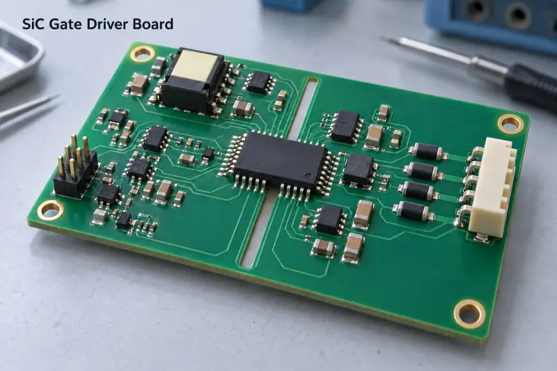
Creepage and clearance requirements depend on the insulation design, voltage conditions, environment and material properties. Copper, vias and other conductive features must respect defined isolation zones on every relevant layer, and slots must retain their approved geometry. Fabrication review can identify a conflict between the design and manufacturing process, but any change to isolation-related geometry needs approval from the design owner.
Tg is the laminate’s glass-transition temperature; it is not a continuous operating-temperature rating. Material selection also needs to account for actual exposure, assembly conditions and the material’s other relevant thermal properties. Conformal coating may suit some environments, but it does not by itself justify reducing creepage or clearance.
Review assembly details before production
DFM review connects the approved layout to a manufacturable and inspectable assembly. It can check trace features against copper thickness and process limits, along with hole and slot dimensions, board edges and copper-to-feature relationships. On densely routed boards, footprint dimensions, component spacing, polarity marks and exposed-pad arrangements also affect how reliably the board can be assembled and inspected.
Panelization and board handling deserve attention near connectors and edge-mounted components. Tooling access, board support and depaneling locations can affect handling during production. Inspection planning should account for visible solder joints, hidden connections and access to designated test points.
Gate-loop geometry, Kelvin-source connections and protection timing are electrical design matters. If a manufacturing change touches one of these areas, it should go back to the design owner for review. Treating it as a routine production adjustment could change the behavior the circuit is intended to deliver.
Coordinate sourcing, assembly and inspection
EBest Circuit supports turnkey, partial-turnkey and consigned assembly, using surface-mount technology (SMT), through-hole processes, or a mix of both. Components can be sourced against the approved BOM, with incoming material checks. Any proposed substitution requires approval before use; footprint compatibility alone does not establish that an alternative part is electrically equivalent.
SMT assembly can include stencil printing, solder paste inspection (SPI), component placement and reflow soldering. Reflow profiling is set for the actual assembly. Through-hole connectors and leaded components use the selected soldering process. The assembly plan needs to match the component mix and board design.
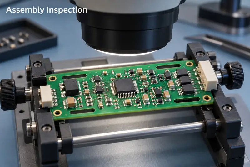
Inspection methods cover different failure modes. Three-dimensional SPI checks solder paste deposition before placement, including its volume, area and height. Automated optical inspection (AOI) can detect missing components, polarity issues and visible solder defects. X-ray inspection can assess hidden joints, including applicable BGA and bottom-terminated packages, where visual inspection cannot reach the connection.
Documented equipment includes bare-board electrical testers, flying-probe equipment, 3D SPI, 3D AOI and an AX8200 X-ray inspection system. Bare-board electrical testing checks for opens and shorts against the board’s electrical data before assembly. First-article inspection checks component values, placement and assembly conformity during initial setup. Visual checks can take place at incoming, in-process and final stages.
Agreed functional testing uses the project’s test procedure, fixtures, equipment and acceptance criteria. SPI, AOI and X-ray each provide useful manufacturing evidence, but none alone demonstrates that the complete SiC switching stage meets its operating specification.
Define system validation as a separate scope
High-voltage insulation testing, double-pulse testing and short-circuit protection validation are not assumed to be part of standard assembly. If the project requires them, the facilities, procedures and responsibilities need to be confirmed separately. This distinction helps make clear what a board-level production inspection establishes and what still needs validation at the electrical system level.
Cost and schedule follow the full build scope
Quotation and lead time depend on the PCB construction as well as the components and production work. Availability of the selected driver ICs, isolated power supplies and protection components can affect purchasing schedules. Higher-CTI materials, extra layers or special processing may affect material availability and fabrication routing. Tight slot, hole or outline tolerances can require additional process review, particularly when a board mates directly with a power module or connector assembly.
Mixed SMT and through-hole assembly, hidden-joint inspection and extra handling steps all contribute to production effort. Dedicated fixtures or new functional test procedures require setup, especially for an initial build. Prototype and repeat-production quantities spread setup costs differently, while component purchasing quantities also affect unit cost.
A useful quotation compares the same scope across suppliers: fabrication, procurement, assembly, inspection and agreed testing. A lower unit price may reflect a narrower inspection or test plan, so those elements need to be clear alongside the board price.
Prepare a complete manufacturing package
For a review and quotation, send the PCB files, drill data and board drawing, along with the BOM, placement data and assembly drawings. Identify the layer stackup, material, copper thickness, surface finish and critical dimensional tolerances. State the build quantity, whether components will be turnkey or customer-supplied, and the required delivery date. Include project-specific acceptance criteria, functional procedures and fixture requirements.
Revision control matters: the files, BOM and assembly data should identify the same approved version. If a driver IC becomes unavailable, a proposed replacement needs design review because it can affect drive characteristics, protection behavior or isolation specifications. Likewise, boards with multiple component variants need clear BOMs, unpopulated-position lists and test configurations for each build.
Gate-drive voltage is device-specific. The selected MOSFET’s recommended drive levels and absolute gate-voltage limits determine the appropriate driver supply and associated components; one voltage setting cannot be assumed to suit every SiC device.
For a manufacturing review, email [email protected] with the PCB package, BOM, quantities and testing scope. The key early decision is whether the proposed construction, assembly plan and inspection criteria all match the approved design.