EBest Circuit to Show PCB Assembly Capabilities at electronica 2026
- Love PCB
- 861 reads
EBest Circuit plans to show PCBA samples in Munich, with discussions spanning board fabrication, sourcing, inspection and production.
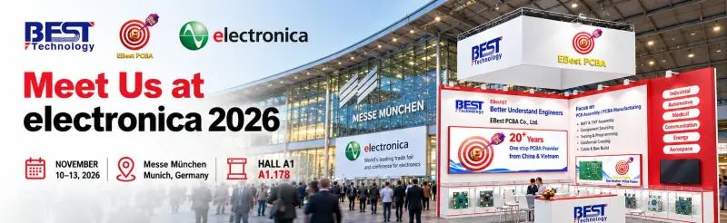
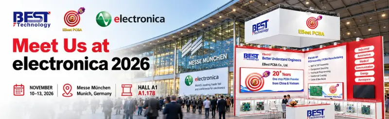
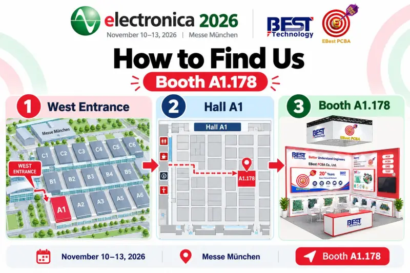
PCB assembly will be the focus of EBest Circuit’s stand at electronica 2026, where visitors can examine assembled board samples and discuss manufacturing requirements with the company’s team. The exhibition runs November 10–13 at Messe München in Munich, Germany; EBest Circuit will be at Hall A1, Booth 178.
The company says its offering covers PCB fabrication, component sourcing, assembly, inspection, testing and further integration. For engineers evaluating a supplier, the useful question is how those steps fit together on a particular design: material choice, board construction, component availability and test requirements can all shape the manufacturing plan.
Assembly examples and process scope
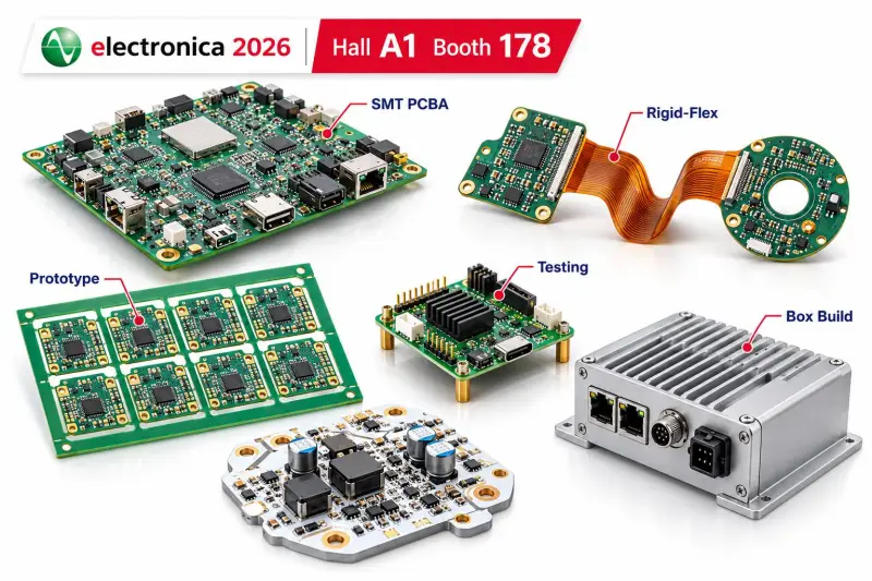
EBest Circuit plans to bring assembled boards representing different structures, component packages, placement densities, connectors and production needs. The stated assembly scope includes SMT, through-hole and mixed SMT/THT work, along with double-sided boards, flexible and rigid-flex circuits, metal-core boards, and assemblies using BGA, QFN and fine-pitch packages.
The company also lists prototype and engineering builds, low- and medium-volume work, and volume production. Related services include turnkey component sourcing, AOI and X-ray inspection, ICT and functional testing, programming, conformal coating, cable assembly and box-build work.
Those options address different manufacturing constraints. A board with BGA devices may need X-ray inspection to examine solder joints that are hidden from a direct view. A power board can bring thermal and current-carrying requirements into the fabrication and assembly discussion. Prototypes may call for flexibility as designs change, while repeat production depends on keeping files, components and process requirements under control.
Board technologies and reference parameters
Because assembly starts with a bare board, EBest Circuit says visitors can discuss PCB fabrication alongside PCBA. Its listed technologies cover several common design pressures, from routing density and signal integrity to heat transfer and mechanical packaging. The following values are company-provided reference parameters; actual requirements depend on the design.
- Multilayer PCB: typically 4–20+ layers and 1–2 oz copper, with controlled impedance available for denser routing.
- HDI PCB: microvias of Ø0.10–0.15 mm, laser-drilled vias, 1+N+1 or 2+N+2 structures, and via-in-pad options.
- Flexible PCB: typically 1–6 layers with 12.5–50 μm PI, for lightweight or space-limited designs, including static and dynamic bend requirements.
- Rigid-flex PCB: typically 4–12+ total layers, including 1–4 flex layers, with controlled bend areas and impedance options.
- Metal-core PCB: 1.0–3.0 mm aluminum or copper cores and thermal conductivity typically in the 1–8 W/m·K range, depending on material.
- Heavy copper PCB: typically 3–10 oz copper, with thicker copper available for project-specific power needs.
- High-Tg PCB: typically Tg ≥170°C for applications with higher thermal requirements.
- High-frequency PCB: Rogers/PTFE or other low-loss laminates, with controlled Dk/Df and RF impedance.
- High-speed and impedance-controlled PCB: controlled 50 Ω single-ended or 90–100 Ω differential impedance; common impedance references include 50 Ω, 90 Ω and 100 Ω, with typical tolerance of ±10% depending on design.
- Ceramic PCB: Al₂O₃ or AlN substrates, with thermal conductivity from about 20 to 170 W/m·K depending on material.
Following fabrication, the listed process path can include component sourcing, stencil preparation, SMT and THT assembly, AOI, X-ray, programming, functional testing, coating, cable assembly and box build. Considering board and assembly requirements together can help surface constraints tied to dense placement, special materials, thermal management, impedance or test access before production begins.
Preparing for a project discussion
Visitors with an active design can bring whatever documentation is available: Gerber files, a BOM, pick-and-place data, PCB or assembly drawings, stack-up details, mechanical drawings, production quantities, and testing or programming requirements. Existing PCBA samples may also help explain construction or assembly concerns.
A finalized production package isn’t required to start a conversation. For a prototype-stage project, the team says it can discuss what further information may be needed for quotation and manufacturing review. A BOM and estimated quantities can anchor sourcing questions; Gerbers, board drawings and assembly data can make engineering discussions more specific.
Face-to-face conversations can also clarify information that may not be evident from files alone. A BOM identifies a component, for example, but may not explain why an alternative is unacceptable. A drawing can locate a connector without stating whether its alignment to an enclosure is critical. Those details can affect sourcing, assembly planning, inspection, testing and production consistency.
Topics EBest Circuit identifies for discussion include stack-up and materials, panelization, assembly constraints, long-lead-time or obsolete components, prototype changes, first-article checks, BGA and fine-pitch assembly, test fixtures, and transfer from prototype to repeat production. Further integration options include coating, mechanical assembly, cable work and box build.
Quality controls and exhibition details
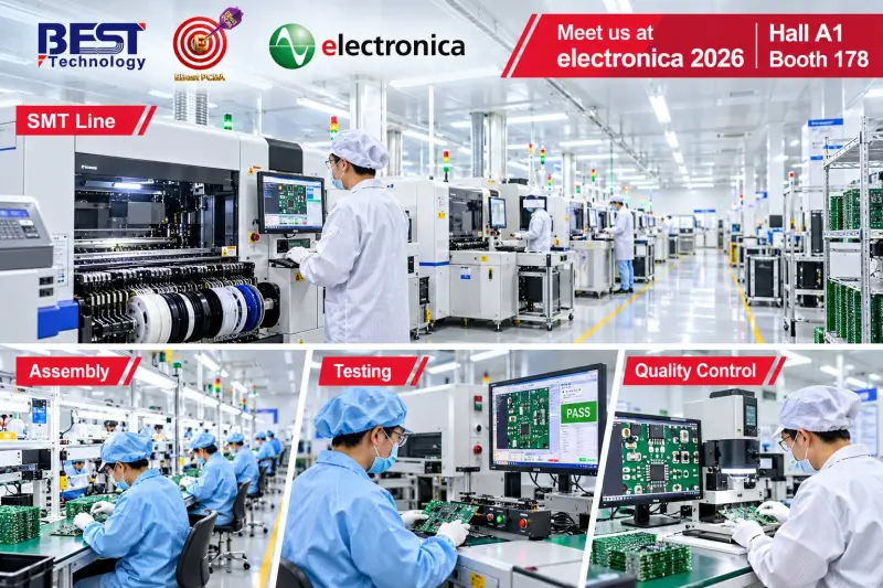
EBest Circuit lists ISO 9001, ISO 13485, IATF 16949, AS9100D, UL, RoHS, REACH and SGS among its certifications and compliance capabilities. It describes manufacturing controls that may include incoming material checks, production records, solder paste inspection, SMT process control, AOI, X-ray, electrical and functional testing, traceability and final inspection. Which controls apply depends on the product and its requirements.
Visitor hours are 09:00–18:00 on November 10, 11 and 12, and 09:00–15:00 on November 13. Visitors who want to discuss a specific project can arrange a meeting at Hall A1, Booth 178. Project files can also be sent to [email protected] before the exhibition.
For engineers comparing manufacturing approaches, the stand offers a chance to review physical PCBA samples and connect board specifications with sourcing, assembly and test questions. Bringing the available design data should make that conversation more concrete.