Reference Designs Reduce Circuit Risk, but BOMs and Layouts Still Need Review
- oliver-freeman
- 834 reads
Reference designs can shorten circuit development by supplying tested topology and layout examples, while leaving system fit and component lifecycle checks to the engineer.
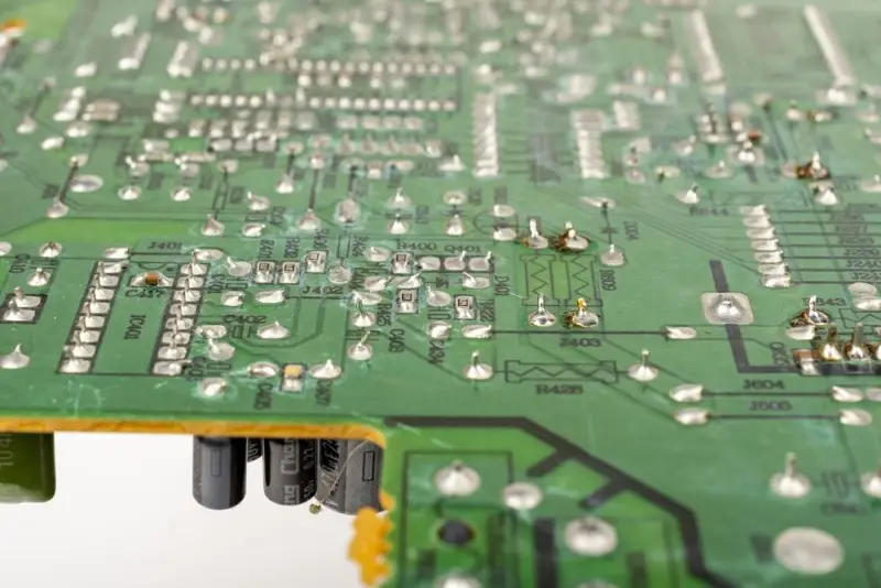
A reference design can move evidence about circuit architecture earlier in development, when changing course is cheaper. Its value is practical: engineers can start with a topology, component pairing and layout that have already been built, then spend their effort checking what must change for the target system. It remains a starting point. The design’s test conditions, parts and physical constraints may not match the product being developed.
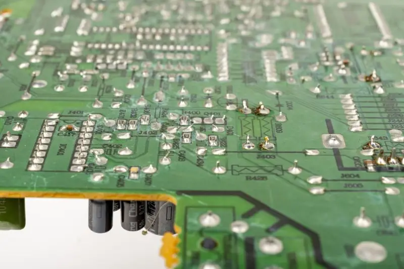
Early architecture choices shape cost and schedule
Kearney reports that up to 80% of product cost is determined during the design phase. Early choices affect component cost, manufacturing difficulty and development time, often before the team has much evidence about how the complete system will behave.
A board built entirely from scratch requires engineers to establish each connection and verify each design decision. If a problem requires a PCB respin, one estimate puts the average cost at $28,500 and the schedule impact at 16 days. The same study reports 2.9 respins per PCB design project. Those figures illustrate why finding architectural or layout problems before routing can matter: repeated respins can consume substantial budget and time.
A reference design doesn’t remove that risk. It provides an existing implementation to inspect before committing to a layout. Engineers can compare its topology and bill of materials (BOM) with their own requirements, while identifying which assumptions need further validation.
A 24 V sensor node: two starting points
Consider a 24 V industrial sensor node with an isolated RS-485 interface. Starting with a blank design means defining the inputs and outputs, then comparing transceivers, digital isolators and isolated DC-DC converters across separate datasheets. The engineer may find parts that look compatible on paper, but still have to establish whether the combination works in the intended circuit.
Part selection then rests on datasheet parameters alone. Passive values and protection circuits need to be calculated, and the layout team must decide how to place the isolated power and data paths while meeting the design’s clearance and creepage requirements. A board might power up successfully on the bench yet show radiated emissions during EMC pre-compliance testing. In the example, switching noise from the isolated DC-DC converter couples into the RS-485 pair. A layout issue of this kind may require a new board spin.

With a published isolated RS-485 reference design, the transceiver, digital isolator and isolated converter have already been paired in hardware. If the design includes test results, those give engineers evidence of its behavior under the stated conditions. The reference schematic supplies a worked topology and component values to adapt for the target load; manufacturer Gerber files can also show how the board handles the isolation gap and thermal vias.
The work shifts rather than disappears. Engineers still define the 24 V input and interface requirements. They review the supplied BOM for lifecycle status and distributor availability, adjust power ratings to match the load, and confirm whether the example’s physical implementation suits their board. A proven power stage can make the first build more informed, but it does not guarantee that a complete product will pass its own tests.
Search for the uncertain block
A reference board that matches an entire product is uncommon. That’s rarely a reason to abandon the approach. A project can draw on several designs: an isolation barrier from an RS-485 interface example, input protection from an industrial power design, and connector spacing or creepage guidance from another board.
The useful question is which block carries the most uncertainty, and whether someone has already built that part. This directs the search toward specific engineering problems instead of requiring a published board that matches every product constraint. It also makes the limits of each borrowed block easier to track.
Three useful roles for a reference design
A development accelerator
Topology, passive values and protection circuits often account for substantial design effort. Starting with a worked implementation lets engineers adapt those choices to their input range and load, instead of deriving every value from scratch. This is where a reference design is most directly useful.

An architecture check
A manufacturer’s design that combines the selected transceiver, isolator and isolated converter is evidence that the parts can operate together under that design’s conditions. That can expose an architecture problem earlier than discovering it during board bring-up. It isn’t a sign-off for another product: load profile, ambient conditions and supply impedance may differ.
A component shortlist
A reference BOM is a useful way to narrow component choices, but it doesn’t ensure future availability. Parts can become not recommended for new designs (NRND) or obsolete, including secondary ICs and passives. Z2Data reports that more than 620,000 electronic parts were discontinued in 2025, often without a formal product change notification. Check lifecycle status and distributor count for every BOM line, especially when the design is several years old.
Adapt the design to the product
Reference designs reflect somebody else’s constraints and priorities. The original board may not fit the product enclosure or meet its thermal limits, so engineers must reassess component placement and layout for their own conditions. A board designed to demonstrate an IC or simplify bench probing may include trade-offs that don’t suit production cost or form factor.
Fabrication details also matter. A layout is useful only if its layer count, dielectric and controlled-impedance requirements can be built by the intended fabricator. Compare those details with available fabrication options before adopting the placement as a starting point. Reference boards may also include test points, extra headers and debug jumpers that need review for a production version.
These checks apply even when the circuit block itself looks like a good fit. A copied design can carry forward unnecessary parts, mismatched thermal assumptions or a stackup the product team can’t reproduce. The goal is to understand what the reference demonstrates and what still needs to be established for the application.
Choosing and using reference designs
It’s usually worth searching for a reference design; whether to start from one depends on where the project’s risk sits. The payoff tends to be greater for blocks involving isolation, high-speed interfaces, switching power or RF, where component interaction and layout carry significant design uncertainty. For a simple LED driver, finding and evaluating an example may take longer than deriving the circuit.
Silicon-vendor designs are valuable for checking a specific IC, since the chip maker tests its own component. Third-party designs can show how parts from different suppliers work together in a more production-like system. Which is more useful depends on what the engineer needs to validate.
Commercial use is often permitted, but the design files’ specific licensing terms still need review before production. Terms can range from open hardware licenses such as CERN-OHL or MIT to more restrictive proprietary conditions.
A reference design is best treated as evidence and a head start: reuse the blocks that answer real uncertainties, then verify their fit, fabrication requirements and component availability against the product. That review is what turns someone else’s board into a defensible starting point for your own.