Wolverhampton Tests Beam Shaping for Tungsten and Metal 3D Printing
- Michael Petch
- 927 reads
A 1.2 kW laser system lets Wolverhampton study how beam profiles affect difficult metals and whether printed thermal components can move from prototype to production.

A single laser-melted track of tungsten has given the University of Wolverhampton a useful research question: how does changing the beam’s energy profile affect the materials and interfaces that metal 3D printing can produce? The early result was an unexpected melt pool. The team hasn’t yet established what that means for finished parts, but the experiment points to the work planned for its new Centre of Excellence for Shaped Laser Additive Manufacturing.

John Robinson, the university’s Additive Manufacturing Research Commercialisation Manager, saw the tungsten samples while reviewing a doctoral researcher’s work. Each sample contained a single track melted across a powder bed. As the team varied the beam profile to distribute energy over a wider area, one setting produced what Robinson described as “a nice melt pool, which I wouldn’t have predicted”. He cautioned that the tests were preliminary: the researchers had not yet compared finished components against parts made on a conventional system.
Building on laser powder bed fusion
The university considered adding binder jetting or cold spray to its Springfield Campus facility, but space was limited. Wolverhampton has worked with laser powder bed fusion since installing an EOS M250 in 1999. Its new direction is to explore what a laser that shapes energy delivery can do within a process the team already understands.
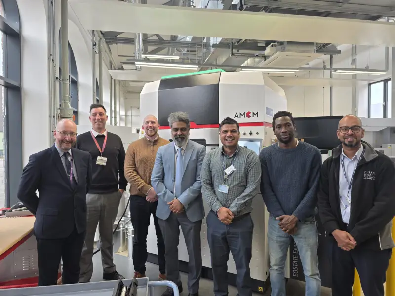
After the M250, the university added an M270 and a 400 W M290. Developed with EOS and AMCM and supported in part by the Regional Innovation Fund, the Springfield centre now has a 1.2 kW AMCM system equipped with an nLIGHT beam-shaping laser. A wider spot may cover more powder in fewer passes, but Wolverhampton’s central research question is about material behaviour: which metals become practical to process, and how do different materials join at their interfaces?

Single-track tests give researchers a controlled starting point. They vary laser power and scan speed while holding other conditions constant, then repeat the work across the machine’s available beam profiles. The Gaussian setting provides a reference. Separate doctoral projects focus on tungsten and molybdenum; work with an industrial collaborator examines copper-coated diamond, which the group has processed with a conventional Gaussian beam, though with difficulty.
Whether the results can transfer to other machines remains an open question. Wolverhampton meets monthly with nLIGHT and hopes to test its parameters on equipment from other manufacturers that uses the same laser technology. Robinson said the team doesn’t yet know how readily the parameters will transfer.
Thermal management drives the materials work
Robinson’s route into thermal engineering began at Cooksongold, where he worked on additive manufacturing in precious metals. Around 2015 or 2016, a US visitor asked whether the team could make a high-performance heat exchanger for valuable electronics, with metal cost secondary to performance. The request stayed with him after he left the company.
He later funded his own doctorate on laser processing of copper and silver at 400 W or less. Both metals conduct heat well and reflect much of the laser light, making them challenging feedstocks for laser processing. The research asked whether useful thermal components could be made on the machines then available. Since then, the group has developed copper parameters across several power ranges and worked on electric-vehicle cooling plates, vapour chambers and a photon absorber for Diamond Light Source.
The photon absorber, developed with Diamond Light Source and the UK Astronomy Technology Centre, shows both the design freedom and the pumping trade-offs of printed cooling channels. One copper design combined 21 individually brazed pipes into a single manifold. Simulations predicted an 11% reduction in maximum temperature compared with the conventional design, while calculations indicated an 82% reduction in pressure drop. A competing coil design increased calculated pressure drop by 31%. Routing coolant close to a heat source can improve thermal performance, but the resulting path may make the fluid harder to pump.
The team printed two absorber prototypes. The temperature and pressure figures came from simulations and calculations, not reported operating measurements. Before the parts could be used at the synchrotron, the researchers identified further work on surface roughness, porosity and dimensional tolerances. The research was published in the Journal of Synchrotron Radiation.
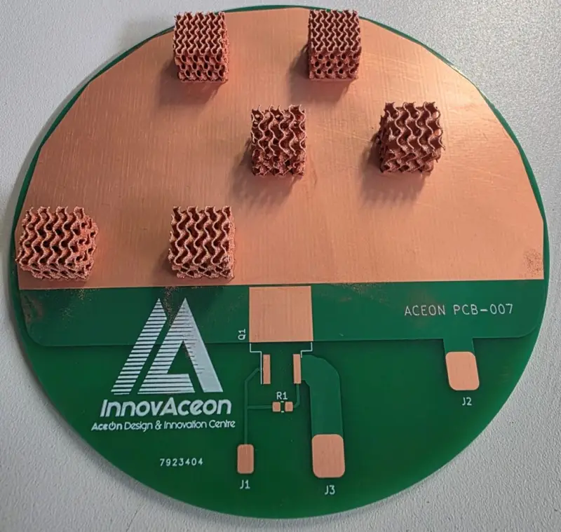
A more recent project, funded by the Henry Royce Institute and conducted with AceOn Group, puts the cooling structure directly on a printed circuit board. Robinson says the team has printed copper heat sinks in several geometries and achieved adhesion. The aim is to remove the thermal interface material typically placed between a board and a separately made heat sink. The practical test is therefore not just whether the copper geometry can be printed, but whether it bonds at the point where heat enters the sink.
A working prototype still needs a route to production
Robinson’s example of a technically successful project that didn’t progress commercially is a functional vapour chamber for electronics cooling. Working with a small company, the team optimised material and geometry parameters, built the chambers and had them tested. The devices worked, but the work stopped before commercial use. Robinson couldn’t identify whether cost or further validation was the deciding factor.
His explanation for the gap is practical: a company already shipping a product has limited time to assess a replacement, and needs a substantial performance gain to justify the change. As he put it, the challenge is “actually proving out the research at a commercial level.”
Springfield is being equipped to support that path from material to tested component. At the time of Robinson’s interview, the AMCM machine was operating, electrical discharge machining equipment had been installed, and CNC capability was being added. The plan is to cover feedstock analysis, printing, machining, and destructive and non-destructive testing. While the centre is being commissioned, its commercial targets are modest; revenue and intellectual property development are intended to sit alongside research publications.
At Formnext, scheduled for 17–20 November 2026, Hall 12.0, Stand F139, the university expects to show copper thermal-management builds, vapour-chamber sections, bismuth telluride and copper-coated diamond samples. Some exhibits represent applications in development; others, like the vapour chamber, demonstrate a working device that still needs a convincing production case. That distinction is central to the centre’s work: beam shaping may expand what can be printed, while component validation and industrial fit will determine what gets used.