Co-Packaged Optics Testing: Scaling Beyond Single-Site Production
- Laura Peters
- 949 reads
Fiber alignment, connector wear and RF probing constrain co-packaged optics testing; multi-site probing and concurrent loopback could increase production throughput.

Fiber alignment remains the main obstacle to scaling optical-engine production tests beyond one device at a time. Multi-site probe cards could raise throughput, but connector durability, radio-frequency access and test time all need attention as co-packaged optics (CPO) and near-packaged optics (NPO) architectures develop.
That’s the picture described by Matt Griffin, senior product manager for optoelectronics test at Teradyne; Ira Leventhal, vice president of research and venture at Advantest America; Dave Armstrong, fellow at ISE Labs, a subsidiary of ASE Group; and Kazuo Yamaguchi, silicon photonics researcher and engineer at Keysight Technologies. Their assessments point to a transition that depends on the device and test insertion: multi-site production is a practical goal for some configurations, while others remain limited by power delivery, contact geometry or optical alignment.

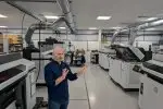
Fig. 1: (L-R): Teradyne’s Griffin; Keysight’s Yamaguchi; ISE Labs’ Armstrong; Advantest’s Leventhal.
Device architecture sets the site count
For a large GPU with a power draw of 8 kW, testing multiple dies at once can be difficult. Armstrong pointed to connectors placed around several sides of the device, alongside the limits on how much power test equipment can deliver to and remove from the part. Those constraints can make a single test site the workable arrangement.
NPO may offer a different path. Armstrong described it as typically a single-connector device, a configuration that will need multi-site testing to support high production volumes. He sees later test insertions, including the second and third, as promising places to increase site count because these stages involve longer and more complex tests. Photonic integrated circuit (PIC) wafer testing, by comparison, is generally single-site today. Armstrong said probe-card capabilities could allow some increase, pointing to work from Technoprobe as a possible sign of progress.
Griffin likewise said most production solutions remain single-site. For optical engines, he identified fiber alignment as the main bottleneck and said multiple companies are working on multi-site approaches. A successful solution could help production scale, but the required technology is still developing.
Connector life is a mechanical design problem
Repeated optical testing should ideally avoid physical contact between the device and either the optical probe or the fiber array unit (FAU). Griffin said that, in a new test system, an FAU can sometimes collide with a device during initial setup. During operation, contamination on the FAU is a more routine concern, making cleaning part of the process.
The device-side connector presents a longer-term challenge. At module level, or on an optical engine with receptacles attached, the connector may be designed for a single attachment that is never undone. Each new connector generation can change both the connector configuration and the automation needed to handle it. That means a design needs to support optical performance while tolerating the handling required during assembly and test.
Leventhal compared the wear issue with repeated socketing of a ball-grid array (BGA), where too many contacts can damage the solder balls. The test-side connector needs a wear-resistant design: it may need to last tens of thousands of insertions, or as many as 100,000, while some device-side receptacles may be less durable. A hardened test connector can itself damage a softer receptacle if the materials and contact arrangement are poorly matched. Connector designs therefore need to balance long test-side life with protection of the device-side interface.
RF access complicates simultaneous testing
Making electrical and optical contacts at the same time is more demanding when the test must characterize high-frequency behavior. Yamaguchi said that modulators and photodetectors are ultimately evaluated using S-parameters, which requires optical access alongside high-frequency RF contact. Probe cards have limited space for RF lines, and their bandwidth is constrained, while devices are characterized above 200 GHz. At wafer and die test stages, he said, simultaneous connection is fundamentally an RF probing challenge.
Package warpage adds another source of difficulty. Leventhal said the contact system must accommodate alignment across multiple axes, including approaches from the top or side. A BGA’s large number of pins also makes reliable contact harder to achieve. Combining those electrical requirements with optical interfaces and the varied layouts of CPO devices increases the complexity of a test system intended to serve multiple architectures.
Griffin noted that interfaces can sit on the top, bottom or both sides of a device. At module level, they may appear across two to four package sides, depending on the number of optical engines. Optical alignment on its own may be manageable; building a scalable system that accommodates these different layouts is the harder task.
Concurrent loopback could reduce test time
Armstrong, who chairs the IPSR photonics test roadmap, said the group’s latest report highlights a methodology for AC testing. Bit error rate testing is among the potential time sinks. With suitable design for test (DFT), a system could run loopback on the optical and electrical sides simultaneously. Today, test setups often run loopback on one side and a bit error rate test on the other, which Armstrong said can double effective test time by requiring an expensive setup.
Concurrent tests could reduce that burden, though the automation work remains. Griffin expects customers moving to volume production to use some form of loopback, whether electrical, optical or combined. Which approach becomes common is still unsettled.
Production metrics must predict integration performance
Insertion loss draws attention because it is measured frequently, but Armstrong said it shouldn’t automatically rank as the leading production concern. He put eye quality first, with high-quality receiver sensitivity and bit error rate also high on the list. Griffin added wavelength sweeps for optical engines, which can consume significant time depending on customer requirements.
Yamaguchi stressed that measurements need to distinguish a known-good die from a known-good and reliable die. A device can pass before assembly and still develop problems during integration or service. Examples include added coupling loss after fiber or FAU attachment, resonance drift relative to laser tunability, and thermal or packaging effects. Transmitter and receiver performance is assessed against standards, using metrics such as TDECQ (Transmitter and Dispersion Eye Closure Quaternary) and receiver sensitivity.
Leventhal said production testing also needs to help identify the cause when data transmission fails in either direction: electrical to optical or optical to electrical. Collecting useful diagnostic information early can make that root-cause work more effective. For higher-volume CPO and NPO production, the practical gains will depend on solving alignment and connector wear while bringing more measurements into the same test sequence.